SBASAB2A February 2022 – July 2022 AMC23C12
PRODUCTION DATA
- 1 Features
- 2 Applications
- 3 Description
- 4 Revision History
- 5 Pin Configuration and Functions
-
6 Specifications
- 6.1 Absolute Maximum Ratings
- 6.2 ESD Ratings
- 6.3 Recommended Operating Conditions
- 6.4 Thermal Information
- 6.5 Power Ratings
- 6.6 Insulation Specifications
- 6.7 Safety-Related Certifications
- 6.8 Safety Limiting Values
- 6.9 Electrical Characteristics
- 6.10 Switching Characteristics
- 6.11 Timing Diagrams
- 6.12 Insulation Characteristics Curves
- 6.13 Typical Characteristics
- 7 Detailed Description
- 8 Application and Implementation
- 9 Device and Documentation Support
- 10Mechanical, Packaging, and Orderable Information
Package Options
Mechanical Data (Package|Pins)
- DWV|8
Thermal pad, mechanical data (Package|Pins)
Orderable Information
3 Description
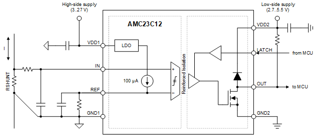
The AMC23C12 is an isolated window comparator with a short response time. The open-drain output is separated from the input circuitry by an isolation barrier that is highly resistant to magnetic interference. This barrier is certified to provide reinforced galvanic isolation of up to 5 kVRMS according to VDE 0884-17 and UL1577, and supports a working voltage of up to 1 kVPK.
The comparison window is centered around 0 V, meaning that the comparator trips if the absolute value of the input voltage exceeds the trip threshold value. The trip threshold is adjustable from 20 mV to 300 mV through a single external resistor and, therefore, the comparison window ranges from ±20 mV to ±300 mV. When the voltage on the REF pin is greater than 550 mV, the negative comparator is disabled and only the positive comparator is functional. The reference voltage in this mode can be as high as 2.7 V. This mode is particularly useful for monitoring voltage supplies.
The open-drain output on the device supports transparent mode (LATCH input tied to GND2) where the output follows the input state, or latch mode, where the output is cleared on the falling edge of the latch input signal.
The AMC23C12 is available in a 8-pin, wide-body SOIC package and is specified over the extended industrial temperature range of –40°C to +125°C.
| PART NUMBER | PACKAGE | BODY SIZE (NOM) |
|---|---|---|
| AMC23C12 | SOIC (8) | 5.85 mm × 7.50 mm |
 Typical Application