SBASA73A July 2020 – May 2021 AMC3301-Q1
PRODUCTION DATA
- 1 Features
- 2 Applications
- 3 Description
- 4 Revision History
- 5 Pin Configuration and Functions
-
6 Specifications
- 6.1 Absolute Maximum Ratings
- 6.2 ESD Ratings
- 6.3 Recommended Operating Conditions
- 6.4 Thermal Information
- 6.5 Power Ratings
- 6.6 Insulation Specifications
- 6.7 Safety-Related Certifications
- 6.8 Safety Limiting Values
- 6.9 Electrical Characteristics
- 6.10 Switching Characteristics
- 6.11 Timing Diagram
- 6.12 Insulation Characteristics Curves
- 6.13 Typical Characteristics
- 7 Detailed Description
- 8 Application and Implementation
- 9 Power Supply Recommendations
- 10Layout
- 11Device and Documentation Support
- 12Mechanical, Packaging, and Orderable Information
Package Options
Mechanical Data (Package|Pins)
- DWE|16
Thermal pad, mechanical data (Package|Pins)
Orderable Information
7.3.2 Data Isolation Channel Signal Transmission
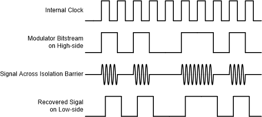
The AMC3301-Q1 uses an on-off keying (OOK) modulation scheme, as shown in Figure 7-1, to transmit the modulator output bitstream across the capacitive SiO2-based isolation barrier. The transmit driver (TX) shown in the Section 7.2 transmits an internally generated, high-frequency carrier across the isolation barrier to represent a digital one and does not send a signal to represent a digital zero. The nominal frequency of the carrier used inside the AMC3301-Q1 is 480 MHz.
The receiver (RX) on the other side of the isolation barrier recovers and demodulates the signal and produces the output. The AMC3301-Q1 transmission channel is optimized to achieve the highest level of common-mode transient immunity (CMTI) and lowest level of radiated emissions caused by the high-frequency carrier and RX/TX buffer switching.
 Figure 7-1 OOK-Based
Modulation Scheme