SNVSBB0A May   2019  – November 2019 ATL431LI-Q1 , ATL432LI-Q1

PRODUCTION DATA.  

  1. Features
  2. Applications
  3. Description
    1.     Device Images
      1.      Simplified Schematic
  4. Revision History
  5. Device Comparison Table
  6. Pin Configuration and Functions
    1.     Pin Functions
  7. Specifications
    1. 7.1 Absolute Maximum Ratings
    2. 7.2 ESD Ratings
    3. 7.3 Recommended Operating Conditions
    4. 7.4 Thermal Information
    5. 7.5 Electrical Characteristics
    6. 7.6 Typical Characteristics
  8. Parameter Measurement Information
    1. 8.1 Temperature Coefficient
    2. 8.2 Dynamic Impedance
  9. Detailed Description
    1. 9.1 Overview
    2. 9.2 Functional Block Diagram
    3. 9.3 Feature Description
    4. 9.4 Device Functional Modes
      1. 9.4.1 Open Loop (Comparator)
      2. 9.4.2 Closed Loop
  10. 10Applications and Implementation
    1. 10.1 Application Information
    2. 10.2 Typical Applications
      1. 10.2.1 Comparator With Integrated Reference
      2. 10.2.2 Design Requirements
      3. 10.2.3 Detailed Design Procedure
        1. 10.2.3.1 Basic Operation
          1. 10.2.3.1.1 Overdrive
        2. 10.2.3.2 Output Voltage and Logic Input Level
          1. 10.2.3.2.1 Input Resistance
      4. 10.2.4 Application Curves
      5. 10.2.5 Precision LED Lighting Current Sink Regulator
        1. 10.2.5.1 Design Requirements
        2. 10.2.5.2 Detailed Design Procedure
          1. 10.2.5.2.1 Basic Operation
            1. 10.2.5.2.1.1 Output Current Range and Accuracy
          2. 10.2.5.2.2 Power Consumption
      6. 10.2.6 Shunt Regulator/Reference
        1. 10.2.6.1 Design Requirements
        2. 10.2.6.2 Detailed Design Procedure
          1. 10.2.6.2.1 Programming Output/Cathode Voltage
          2. 10.2.6.2.2 Total Accuracy
          3. 10.2.6.2.3 Stability
          4. 10.2.6.2.4 Start-Up Time
        3. 10.2.6.3 Application Curves
      7. 10.2.7 Isolated Flyback with Optocoupler
        1. 10.2.7.1 Design Requirements
          1. 10.2.7.1.1 Detailed Design Procedure
            1. 10.2.7.1.1.1 ATL431LI-Q1 Biasing
            2. 10.2.7.1.1.2 Resistor Feedback Network
      8. 10.2.8 Adjustable Reference for Tracking LDO
        1. 10.2.8.1 Design Requirements
        2. 10.2.8.2 Detailed Design Procedure
          1. 10.2.8.2.1 External Capacitors
    3. 10.3 System Examples
  11. 11Power Supply Recommendations
  12. 12Layout
    1. 12.1 Layout Guidelines
    2. 12.2 Layout Example
  13. 13Device and Documentation Support
    1. 13.1 Device Support
      1. 13.1.1 Device Nomenclature
    2. 13.2 Documentation Support
      1. 13.2.1 Related Documentation
    3. 13.3 Related Links
    4. 13.4 Receiving Notification of Documentation Updates
    5. 13.5 Support Resources
    6. 13.6 Trademarks
    7. 13.7 Electrostatic Discharge Caution
    8. 13.8 Glossary
  14. 14Mechanical, Packaging, and Orderable Information

Package Options

Mechanical Data (Package|Pins)
Thermal pad, mechanical data (Package|Pins)
Orderable Information

Parameter Measurement Information

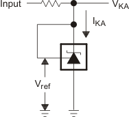
ATL431LI-Q1 ATL432LI-Q1 pmi_vka_eq_vref_lvs543.gifFigure 17. Test Circuit for VKA = Vref
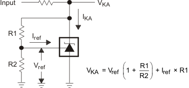
ATL431LI-Q1 ATL432LI-Q1 pmi_vka_gt_vref_lvs543.gifFigure 18. Test Circuit for VKA > Vref
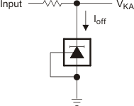
ATL431LI-Q1 ATL432LI-Q1 pmi_ioff_lvs543.gifFigure 19. Test Circuit for Ioff