SWRS188D May 2017 – December 2021 AWR1243
PRODUCTION DATA
- 1 Features
- 2 Applications
- 3 Description
- 4 Functional Block Diagram
- 5 Revision History
- 6 Device Comparison
- 7 Terminal Configuration and Functions
-
8 Specifications
- 8.1 Absolute Maximum Ratings
- 8.2 ESD Ratings
- 8.3 Power-On Hours (POH)
- 8.4 Recommended Operating Conditions
- 8.5 Power Supply Specifications
- 8.6 Power Consumption Summary
- 8.7 RF Specification
- 8.8 Thermal Resistance Characteristics for FCBGA Package [ABL0161]
- 8.9
Timing and Switching Characteristics
- 8.9.1 Power Supply Sequencing and Reset Timing
- 8.9.2 Synchronized Frame Triggering
- 8.9.3 Input Clocks and Oscillators
- 8.9.4 Multibuffered / Standard Serial Peripheral Interface (MibSPI)
- 8.9.5 LVDS Interface Configuration
- 8.9.6 General-Purpose Input/Output
- 8.9.7 Camera Serial Interface (CSI)
- 9 Detailed Description
- 10Monitoring and Diagnostics
- 11Applications, Implementation, and Layout
- 12Device and Documentation Support
- 13Mechanical, Packaging, and Orderable Information
Package Options
Refer to the PDF data sheet for device specific package drawings
Mechanical Data (Package|Pins)
- ABL|161
Thermal pad, mechanical data (Package|Pins)
Orderable Information
8.9.7.1 CSI Switching Characteristics
over operating free-air temperature range (unless otherwise noted)
| PARAMETER | MIN | TYP | MAX | UNIT | ||
|---|---|---|---|---|---|---|
| HPTX | ||||||
| HSTXDBR | Data bit rate | (1/2/4 data lane PHY) | 150 | 600 | Mbps | |
| fCLK | DDR clock frequency | (1/2/4 data lane PHY) | 75 | 300 | MHz | |
| ΔVCMTX(LF) | Common-level variation | –50 | 50 | mV | ||
| tR and tF | 20% to 80% rise time and fall time | 0.3 | UI | |||
| LPTX DRIVER | ||||||
| tEOT | Time from start of THS-TRAIL period to start of LP-11 state | 105 + 12*UI | ns | |||
| DATA-CLOCK Timing Specification | ||||||
| UINOM | Nominal Unit Interval | 1.67 | 13.33 | ns | ||
| UIINST,MIN | Minimum instantaneous Unit Interval | 1.131 | ns | |||
| TSKEW[TX] | Data to clock skew measured at transmitter | –0.15 | 0.15 | UIINST,MIN | ||
| CSI2 TIMING SPECIFICATION | ||||||
| TCLK-PRE | Time that the HS clock shall be driven by the transmitter before any associated data lane beginning the transition from LP to HS mode. | 8 | ns | |||
| TCLK-PREPARE | Time that the transmitter drives the clock lane LP-00 line state immediately before the HS-0 line state starting the HS transmission. | 38 | 95 | ns | ||
| TCLK-PREPARE + TCLK-ZERO | TCLK-PREPARE + time that the transmitter drives the HS-0 state before starting the clock. | 300 | ns | |||
| TEOT | Transmitted time interval from the start of THS-TRAIL or TCLKTRAIL, to the start of the LP-11 state following a HS burst. | 105 ns + 12*UI | ns | |||
| THS-PREPARE | Time that the transmitter drives the data lane LP-00 line state immediately before the HS-0 line state starting the HS transmission | 40 + 4*UI | 85 + 6*UI | ns | ||
| THS-PREPARE + THS-ZERO | THS-PREPARE + time that the transmitter drives the HS-0 state prior to transmitting the Sync sequence. | 145 ns + 10*UI | ns | |||
| THS-EXIT | Time that the transmitter drives LP-11 following a HS burst. | 100 | ns | |||
| THS-TRAIL | Time that the transmitter drives the flipped differential state after last payload data bit of a HS transmission burst | max(8*UI, 60 ns + 4*UI) | ns | |||
| TLPX | TXXXransmitted length of any low-power state period | 50 | ns | |||
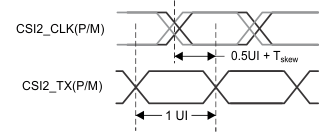
 Figure 8-9 Clock and Data Timing in HS Transmission
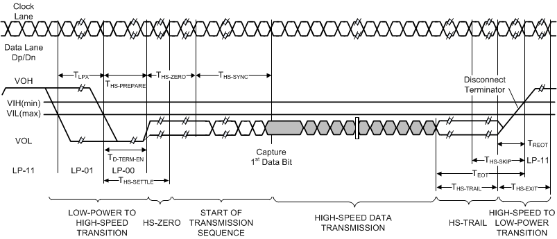
 Figure 8-10 High-Speed Data Transmission Burst
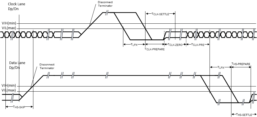
The HS to LP transition of the CLK does not actually take place since the CLK is always ON in HS mode.
Figure 8-11 Switching the Clock Lane Between Clock Transmission and Low-Power Mode