SLUS940D September 2009 – May 2021 BQ24050 , BQ24052
PRODUCTION DATA
- 1 Features
- 2 Applications
- 3 Description
- 4 Revision History
- 5 Pin Configuration and Functions
- 6 Specifications
-
7 Detailed Description
- 7.1 Overview
- 7.2 Functional Block Diagram
- 7.3
Feature Description
- 7.3.1 Power Down, or Undervoltage Lockout (UVLO)
- 7.3.2 Power Up
- 7.3.3 D+, D– Detection
- 7.3.4 New Charge Cycle
- 7.3.5 Overvoltage Protection (OVP) – Continuously Monitored
- 7.3.6 CHG Pin Indication
- 7.3.7 CHG LED Pullup Source
- 7.3.8 Input DPM Mode (VIN-DPM or IN-DPM)
- 7.3.9 OUT
- 7.3.10 ISET
- 7.3.11 TS
- 7.3.12 Termination and Timer Disable Mode (TTDM) -TS Pin High
- 7.3.13 Timers
- 7.3.14 Termination
- 7.3.15 Battery Detect Routine
- 7.3.16 Refresh Threshold
- 7.3.17 Starting a Charge on a Full Battery
- 7.4 Device Functional Modes
- 7.5 Programming
- 8 Application and Implementation
- 9 Power Supply Recommendations
- 10Layout
- 11Device and Documentation Support
Package Options
Mechanical Data (Package|Pins)
- DSQ|10
Thermal pad, mechanical data (Package|Pins)
Orderable Information
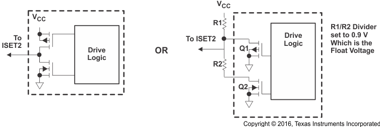
7.5.2 ISET2
Is a 3-state input and programs the Input Current Limit/Regulation Threshold. A low will program a regulated fast charge current via the ISET resistor and is the maximum allowed input/output current for any ISET2 setting, Float will program a 100-mA Current limit and High will program a 500-mA Current limit. Note that initially the D+/D– detection will latch the charge mode according to the source detected (dedicated charger: ISET; USB Host: at 100 mA) until the ISET2 pin has changed states, indicating the processor or transceiver is controlling the pin.
The detection routine registers the input level (Low–High-Z–High) of the ISET2 pin typically 532 μs after applying input power (VIN > 3.4 V – UVLO). After the detection routine is complete, which is typically 100 ms after a pullup on the D+ or D– line or after typically 570 ms if no pullup, the IC monitors the ISET2 pin for a change of state. If the state changes (Low–High-Z–High) from the one registered, for more than 5 μs, then the "detected" latched charge mode is released and is then controlled by the ISET2 pin. The completion of the detection routine varies due to the mechanical-plugging action of the USB cable; therefore, it is best to wait ≥ 600 ms after VIN > 3.4 V to take control of the ISET2 pin.
The following illustration shows two configurations for driving the 3-state ISET2 pin: