SLUS940D September   2009  – May 2021 BQ24050 , BQ24052

PRODUCTION DATA  

  1. Features
  2. Applications
  3. Description
  4. Revision History
  5. Pin Configuration and Functions
  6. Specifications
    1. 6.1 Absolute Maximum Ratings (1)
    2. 6.2 ESD Ratings
    3. 6.3 Recommended Operating Conditions (1)
    4. 6.4 Thermal Information
    5. 6.5 Electrical Characteristics
    6. 6.6 Timing Requirements
    7. 6.7 Switching Characteristics
    8. 6.8 Typical Characteristics
      1. 6.8.1 Power Up, Down, OVP, Disable and Enable Waveforms
      2. 6.8.2 Protection Circuits Waveforms
  7. Detailed Description
    1. 7.1 Overview
    2. 7.2 Functional Block Diagram
    3. 7.3 Feature Description
      1. 7.3.1  Power Down, or Undervoltage Lockout (UVLO)
      2. 7.3.2  Power Up
      3. 7.3.3  D+, D– Detection
      4. 7.3.4  New Charge Cycle
      5. 7.3.5  Overvoltage Protection (OVP) – Continuously Monitored
      6. 7.3.6  CHG Pin Indication
      7. 7.3.7  CHG LED Pullup Source
      8. 7.3.8  Input DPM Mode (VIN-DPM or IN-DPM)
      9. 7.3.9  OUT
      10. 7.3.10 ISET
      11. 7.3.11 TS
      12. 7.3.12 Termination and Timer Disable Mode (TTDM) -TS Pin High
      13. 7.3.13 Timers
      14. 7.3.14 Termination
      15. 7.3.15 Battery Detect Routine
      16. 7.3.16 Refresh Threshold
      17. 7.3.17 Starting a Charge on a Full Battery
    4. 7.4 Device Functional Modes
      1. 7.4.1 Sleep Mode
    5. 7.5 Programming
      1. 7.5.1 PRE_TERM – Precharge and Termination Programmable Threshold
      2. 7.5.2 ISET2
  8. Application and Implementation
    1. 8.1 Application Information
    2. 8.2 Typical Applications
      1. 8.2.1 BQ2405x Charger Application Design Example
        1. 8.2.1.1 Design Requirements
        2. 8.2.1.2 Detailed Design Procedure
          1. 8.2.1.2.1 Program the Fast Charge Current, ISET
          2. 8.2.1.2.2 Program the Termination Current Threshold, ITERM
          3. 8.2.1.2.3 TS Function
          4. 8.2.1.2.4 CHG
          5. 8.2.1.2.5 Selecting IN and OUT Pin Capacitors
        3. 8.2.1.3 Application Curves
  9. Power Supply Recommendations
  10. 10Layout
    1. 10.1 Layout Guidelines
    2. 10.2 Layout Example
    3. 10.3 Thermal Considerations
      1. 10.3.1 Leakage Current Effects on Battery Capacity
  11. 11Device and Documentation Support
    1. 11.1 Device Support
      1. 11.1.1 Third-Party Products Disclaimer
    2. 11.2 Documentation Support
      1. 11.2.1 Related Documentation
    3. 11.3 Receiving Notification of Documentation Updates
    4. 11.4 Support Resources
    5. 11.5 Trademarks
    6. 11.6 Electrostatic Discharge Caution
    7. 11.7 Glossary

Package Options

Mechanical Data (Package|Pins)
Thermal pad, mechanical data (Package|Pins)
Orderable Information

Power Up, Down, OVP, Disable and Enable Waveforms

GUID-7871B2A6-9F1F-4071-BF62-652537B32082-low.gif
.
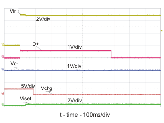
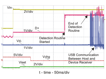
Detected D– line pulled to 0.6 V and the detection routine is started
Figure 6-1 D+ D– Detection for Adaptor Hot Plug
GUID-F38B7D15-EA2B-463C-9598-CBD1F9AFFE0A-low.gif
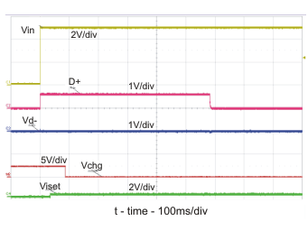
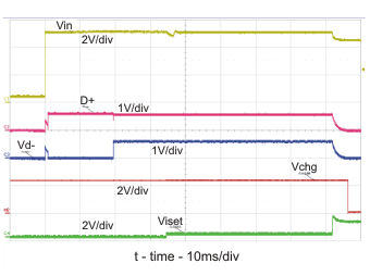
(Device transceiver is "dead") After 500 ms, the detection routine is forced to run.
Figure 6-3 D+ D– Detection for USB Hot Plug No Pullup
GUID-DC8C912E-E734-46AD-8D80-BE6F604F24C3-low.gif
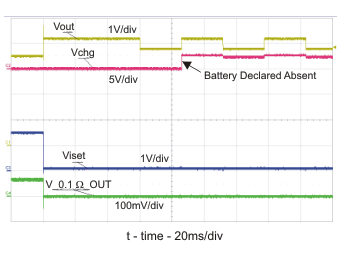
42-Ω Load
Figure 6-5 Battery Removal – GND Removed First
GUID-9E1F8B1F-DF0D-43EB-85F3-AA3178F6DCBD-low.gif
.
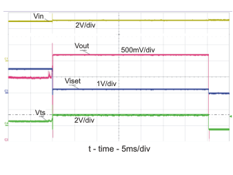
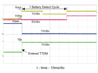
Continuous battery detection when not in TTDM
Figure 6-7 Battery Removal With Fixed TS = 0.5 V
GUID-306B2BD8-CD5D-49FD-8984-6638C31B502D-low.gif
.
No signal detected on D+ or D–. After 500 ms, the detection routine is forced to run
Figure 6-2 D+ D– Detection for Unknown Source Hot Plug
GUID-C67D0FD2-E6E2-418D-BA80-A80273F62C7A-low.gifFigure 6-4 D+ D– Detection for USB Hot Plug With Pullup
GUID-CAA12DC1-C90E-4F3E-981B-7AFBEC9BFB8C-low.gif
100–Ω Load
Figure 6-6 Battery Removal With OUT and TS Disconnect First