SLUSB76B February 2013 – May 2015
PRODUCTION DATA.
- 1 Features
- 2 Applications
- 3 Description
- 4 Revision History
- 5 Description (continued)
- 6 Pin Configuration and Functions
- 7 Specifications
-
8 Detailed Description
- 8.1 Overview
- 8.2 Functional Block Diagrams
- 8.3
Feature Description
- 8.3.1 Input Voltage Protection
- 8.3.2 Battery Protection
- 8.3.3 DEFAULT Mode
- 8.3.4 USB Friendly Power Up
- 8.3.5 Input Current Limiting at Power Up
- 8.3.6 Factory Mode
- 8.3.7 Spread Spectrum Mode
- 8.3.8 PWM Controller in Charge Mode
- 8.3.9 Battery Charging Process
- 8.3.10 Thermal Regulation and Protection
- 8.3.11 Charge Status Output, STAT Pin
- 8.3.12 Control Bits in Charge Mode
- 8.3.13 Control Pins in Charge Mode
- 8.3.14 Boost Mode Operation
- 8.3.15 High Impedance (Hi-Z) Mode
- 8.3.16 Serial Interface Description
- 8.4 Device Functional Modes
- 8.5 Register Maps
- 9 Application and Implementation
- 10Power Supply Recommendations
- 11Layout
- 12Device and Documentation Support
- 13Mechanical, Packaging, and Orderable Information
Package Options
Mechanical Data (Package|Pins)
- YFF|20
Thermal pad, mechanical data (Package|Pins)
Orderable Information
1 Features
- Integrated Power FETs for up to 1.55-A Charge Rate
- Spread Spectrum Frequency Control for Improved EMI Performance
- High-Accuracy Voltage and Current Regulation
- Input Current Regulation Accuracy:
±5% (100 mA and 500 mA) - Charge Voltage Regulation Accuracy:
±0.5% (25°C), ±1% (0°C to 125°C) - Charge Current Regulation Accuracy: ±5%
- Input Current Regulation Accuracy:
- Factory Test-Mode for GSM Calibration Without a Battery
- Input Voltage Based Dynamic Power Management (VIN DPM)
- Bad Adaptor Detection and Rejection
- Safety Limit Register for Maximum Charge Voltage and Current Limiting
- High-Efficiency Mini-USB/AC Battery Charger for Single-Cell Li-Ion and Li-Polymer Battery Packs
- 20-V Absolute Maximum Input Voltage Rating
- 6.5-V Maximum Operating Input Voltage
- Programmable Charge Parameters through I2C Compatible Interface (up to 3.4 Mbps):
- Synchronous Fixed-Frequency PWM Controller Operating at 3 MHz With 0% to 99.5% Duty Cycle
- Automatic High Impedance Mode for Low Power Consumption
- Robust Protection
- Reverse Leakage Protection Prevents Battery Drainage
- Thermal Regulation and Protection
- Input/Output Overvoltage Protection
- Status Output for Charging and Faults
- USB Friendly Boot-Up Sequence
- Automatic Charging
- Power Up System Without Battery
- Boost Mode Operation for USB OTG:
- Input Voltage Range (from Battery):
3.2 to 4.5 V - Output for VBUS: 5.05 V, 350 mA
- Input Voltage Range (from Battery):
- 2.1 × 2.0-mm, 20-Pin DSBGA Package
- Pin-to-Pin Compatible With bq24157 and bq24158
2 Applications
- Mobile and Smart Phones
- MP3 Players
- Handheld Devices
3 Description
The bq24157S is a compact, flexible, high-efficiency, USB-friendly switch-mode charge management device for single-cell Li-ion and Li-polymer batteries used in a wide range of portable applications. The charge parameters can be programmed through an I2C interface. The IC integrates a synchronous PWM controller, power MOSFETs, input current sensing, high-accuracy current and voltage regulation, and charge termination, into a small DSBGA package.
The IC charges the battery in three phases: conditioning, constant current, and constant voltage. The input current is automatically limited to the value set by the host.
Device Information(1)
| PART NUMBER | PACKAGE | BODY SIZE (NOM) |
|---|---|---|
| bq24157S | DSBGA (20) | 2.10 mm × 2.00 mm |
- For all available packages, see the orderable addendum at the end of the data sheet.
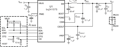
Typical Application Circuit

4 Revision History
Changes from A Revision (June 2014) to B Revision
- Deleted "Safety Timer with Reset Control" from the FeaturesGo
- Changed the package Features From: 2.25 x 2.65 mm To: 2.1 x 2.0 mmGo
- Changed the BODY SIZE values in the Device Information tableGo
- Moved Tstg Storage Temperature From: ESD Ratings To: Absolute Maximum RatingsGo
- Changed the title of Figure 3 From Battery Detection at Power Up To: Power Up in DEFAULT ModeGo
- Changed "32S Mode" To: "HOST Mode" and 15 Minute Mode To: DEFAULT Mode in Figure 5Go
- Changed 32-second mode To: HOST mode in the Overview sectionGo
- Changed 15-minute operation To: default mode in the Overview sectionGo
- Changed 100-ms power-up delay From: No To: Yes in Table 1Go
- Changed Figure 19Go
- Changed text From: "During the normal charging process with HOST control..." To: "During the normal charging process with HOST control and termination enabled.." Go
- Changed Title From: 15-Minute Safety Timer To: DEFAULT ModeGo
- Changed 32-second mode To: HOST mode in USB Friendly Power UpGo
- Changed 15-minute mode To: DEFAULT mode and 32-s mode To: HOST mode in Input Current Limiting at Power UpGo
- Added a NOTE to the Application and Implementation sectionGo
- Changed Figure 30Go
- Changed Figure 31Go
- Added Figure 30Go
Changes from * Revision (February 2013) to A Revision
- Added the Handling Ratings table, Detailed Description section, Feature Description section, Device Functional Modes section, Register Maps section, Application and Implementation section. Power Supply Recommendations section, Layout section, Device and Documentation Support section, Mechanical, Packaging, and Orderable Information sectionGo