SLUSB76B February 2013 – May 2015
PRODUCTION DATA.
- 1 Features
- 2 Applications
- 3 Description
- 4 Revision History
- 5 Description (continued)
- 6 Pin Configuration and Functions
- 7 Specifications
-
8 Detailed Description
- 8.1 Overview
- 8.2 Functional Block Diagrams
- 8.3
Feature Description
- 8.3.1 Input Voltage Protection
- 8.3.2 Battery Protection
- 8.3.3 DEFAULT Mode
- 8.3.4 USB Friendly Power Up
- 8.3.5 Input Current Limiting at Power Up
- 8.3.6 Factory Mode
- 8.3.7 Spread Spectrum Mode
- 8.3.8 PWM Controller in Charge Mode
- 8.3.9 Battery Charging Process
- 8.3.10 Thermal Regulation and Protection
- 8.3.11 Charge Status Output, STAT Pin
- 8.3.12 Control Bits in Charge Mode
- 8.3.13 Control Pins in Charge Mode
- 8.3.14 Boost Mode Operation
- 8.3.15 High Impedance (Hi-Z) Mode
- 8.3.16 Serial Interface Description
- 8.4 Device Functional Modes
- 8.5 Register Maps
- 9 Application and Implementation
- 10Power Supply Recommendations
- 11Layout
- 12Device and Documentation Support
- 13Mechanical, Packaging, and Orderable Information
Package Options
Mechanical Data (Package|Pins)
- YFF|20
Thermal pad, mechanical data (Package|Pins)
Orderable Information
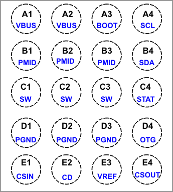
6 Pin Configuration and Functions
20-Bump DSBGA Package
(Top View)

Pin Functions
| PIN | I/O | DESCRIPTION | |
|---|---|---|---|
| NAME | NUMBER | ||
| BOOT | A3 | I/O | Bootstrap capacitor connection for the high-side FET gate driver. Connect a 33-nF ceramic capacitor (voltage rating ≥10 V) from BOOT pin to SW pin. |
| CD | E2 | I | Charge disable control pin. CD = 0, charge is enabled. CD = 1, charge is disabled and VBUS pin is high impedance to GND. |
| CSIN | E1 | I | Charge current-sense input. Battery current is sensed across an external sense resistor. A 0.1-μF ceramic capacitor to PGND is required. |
| CSOUT | E4 | I | Battery voltage and current sense input. Bypass it with a ceramic capacitor (minimum 0.1 μF) to PGND if there are long inductive leads to battery. |
| OTG | D4 | I | Boost mode enable control or input current limiting selection pin. When OTG is in active status, the device is forced to operate in boost mode. It has higher priority over I2C control and can be disabled using the control register. At POR while in DEFAULT mode, the OTG pin is the default to be used as the input current limiting selection pin. The I2C register is ignored at startup. When OTG = High, IIN_LIMIT = 500 mA and when OTG = Low, IIN_LIMIT = 100 mA. |
| PGND | D1, D2, D3 | Power ground | |
| PMID | B1, B2, B3 | I/O | Connection point between reverse blocking FET and high-side switching FET. Bypass it with a minimum of 3.3-μF capacitor from PMID to PGND. |
| SCL | A4 | I | I2C interface clock. Connect a 10-kΩ pullup resistor to 1.8-V rail (VAUX= VCC_HOST) |
| SDA | B4 | I/O | I2C interface data. Connect a 10-kΩ pullup resistor to 1.8-V rail (VAUX= VCC_HOST) |
| STAT | C4 | O | Charge status pin. Pull low when charge in progress. Open drain for other conditions. During faults, a 128-μs pulse is sent out. STAT pin can be disabled by the EN_STAT bit in control register. STAT can be used to drive a LED or communicate with a host processor. |
| SW | C1, C2, C3 | O | Internal switch to output inductor connection |
| VBUS | A1, A2 | I/O | Charger input voltage. Bypass it with a 1-μF ceramic capacitor from VBUS to PGND. It also provides power to the load during boost mode. |
| VREF | E3 | O | Internal bias regulator voltage. Connect a 1-µF ceramic capacitor from this output to PGND. TI does not recommend an external load on VREF. |