SLUSAD2C November 2010 – April 2015
PRODUCTION DATA.
- 1 Features
- 2 Applications
- 3 Description
- 4 Revision History
- 5 Description (continued)
- 6 Device Comparison Table
- 7 Pin Configuration and Functions
- 8 Specifications
-
9 Detailed Description
- 9.1 Overview
- 9.2 Functional Block Diagram
- 9.3
Feature Description
- 9.3.1 Battery Voltage Regulation
- 9.3.2 Battery Current Regulation
- 9.3.3 Battery Precharge Current Regulation
- 9.3.4 Input Current Regulation
- 9.3.5 Charge Termination, Recharge, and Safety Timers
- 9.3.6 Power Up
- 9.3.7 Input Undervoltage Lockout (UVLO)
- 9.3.8 Input Overvoltage/Undervoltage Protection
- 9.3.9 Enable and Disable Charging
- 9.3.10 System Power Selector
- 9.3.11 Converter Operation
- 9.3.12 Automatic Internal Soft-Start Charger Current
- 9.3.13 Charge Overcurrent Protection
- 9.3.14 Charge Undercurrent Protection
- 9.3.15 Battery Detection
- 9.3.16 Battery Short Protection
- 9.3.17 Battery Overvoltage Protection
- 9.3.18 Temperature Qualification
- 9.3.19 MOSFET Short Circuit and Inductor Short Circuit Protection
- 9.3.20 Thermal Regulation and Shutdown Protection
- 9.3.21 Timer Fault Recovery
- 9.3.22 Inductor, Capacitor, and Sense Resistor Selection Guidelines
- 9.3.23 Charge Status Outputs
- 9.4 Device Functional Modes
- 10Application and Implementation
- 11Power Supply Recommendations
- 12Layout
- 13Device and Documentation Support
- 14Mechanical, Packaging, and Orderable Information
Package Options
Mechanical Data (Package|Pins)
- RGY|24
Thermal pad, mechanical data (Package|Pins)
- RGY|24
Orderable Information
9 Detailed Description
9.1 Overview
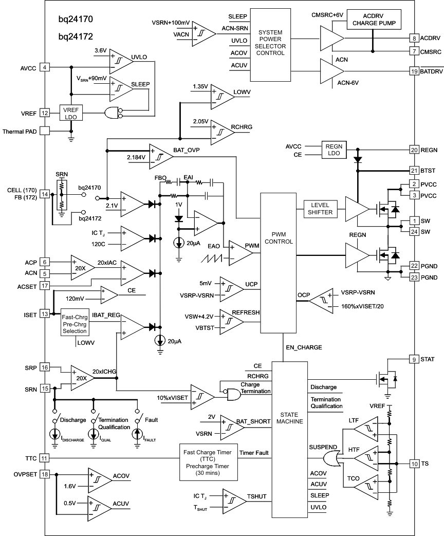
The bq2417x device is a stand-alone switched-mode battery charger for Li-ion and Li-Polymer batteries with power path management and integrated N-channel power MOSFETs. This fixed-frequency synchronous PWM charger offers high accuracy regulation of input current charge current and battery regulation voltage.
9.2 Functional Block Diagram
9.3 Feature Description
Figure 14 shows a typical charging profile.
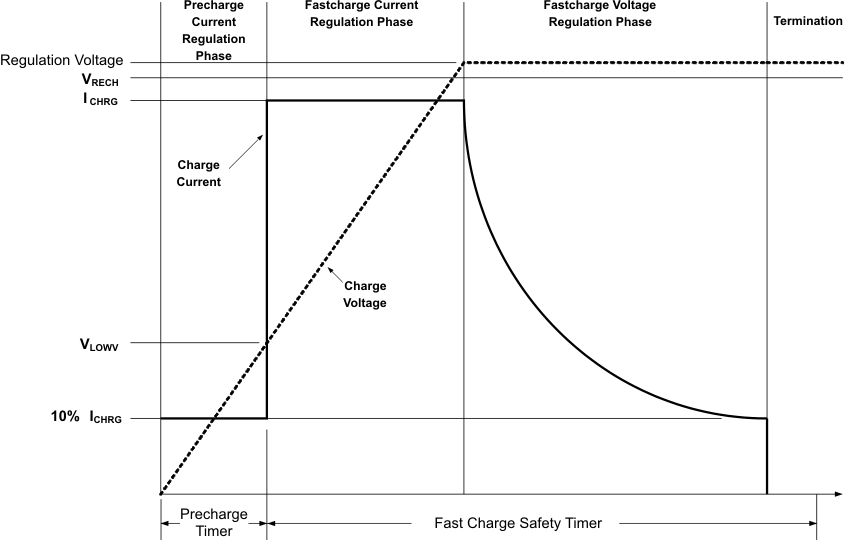 Figure 14. Typical Charging Profile
9.3.1 Battery Voltage Regulation
The bq2417x offers a high-accuracy voltage regulator on for the charging voltage. The bq24170 uses CELL pin to select number of cells with a fixed 4.2 V/cell. Connecting CELL to AGND sets 1-cell output, floating CELL pin sets 2-cell output, and connecting to VREF sets 3-cell output.
Table 2. bq24170 CELL Pin Settings
| CELL PIN | VOLTAGE REGULATION |
|---|---|
| AGND | 4.2 V |
| Floating | 8.4 V |
| VREF | 12.6 V |
The bq24172 uses external resistor divider for voltage feedback and regulate to internal 2.1-V voltage reference on FB pin. Use the following equation for the regulation voltage for bq24172:

where
- R2 is connected from FB to the battery.
- R1 is connected from FB to GND.
9.3.2 Battery Current Regulation
The ISET input sets the maximum charging current. Battery current is sensed by current sensing resistor RSR connected between SRP and SRN. The full-scale differential voltage between SRP and SRN is 40 mV maximum. The equation for charge current is:

The valid input voltage range of ISET is up to 0.8 V. With 10-mΩ sense resistor, the maximum output current is
4 A. With 20-mΩ sense resistor, the maximum output current is 2 A.
The charger is disabled when the ISET pin voltage is below 40 mV and is enabled when ISET pin voltage is above 120 mV. For 10-mΩ current sensing resistor, the minimum fast charge current must be higher than 600 mA.
Under high ambient temperature, the charge current will fold back to keep IC temperature not exceeding 120°C.
9.3.3 Battery Precharge Current Regulation
On power up, if the battery voltage is below the VLOWV threshold, the bq2417x applies the precharge current to the battery. This precharge feature is intended to revive deeply discharged cells. If the VLOWV threshold is not reached within 30 minutes of initiating precharge, the charger turns off and a FAULT is indicated on the status pins.
For bq2417x, the precharge current is set as 10% of the fast charge rate set by ISET voltage.

9.3.4 Input Current Regulation
The total input current from an AC adapter or other DC sources is a function of the system supply current and the battery charging current. System current normally fluctuated as portions of the systems are powered up or down. Without Dynamic Power Management (DPM), the source must be able to supply the maximum system current and the maximum available charger input current simultaneously. By using DPM, the input current regulator reduces the charging current when the summation of system power and charge power exceeds the maximum input power. Therefore, the current capability of the AC adapter can be lowered, reducing system cost.
Input current is set by the voltage on ACSET pin using the following equation:

The ACP and ACN pins are used to sense across RAC with default value of 10 mΩ. However, resistors of other values can also be used. A larger sense resistor will give a larger sense voltage and higher regulation accuracy, at the expense of higher conduction loss.
9.3.5 Charge Termination, Recharge, and Safety Timers
The charger monitors the charging current during the voltage regulation phase. Termination is detected when the SRN voltage (bq24170) or FB voltage (bq24172) is higher than recharge threshold and the charge current is less than the termination current threshold, as calculated in Equation 5:

where
- VISET is the voltage on the ISET pin.
- RSR is the sense resistor.
There is a 25-ms deglitch time during transition between fast charge and precharge.
As a safety backup, the charger also provides an internal fixed 30-minute precharge safety timer and a programmable fast charge timer. The fast charge time is programmed by the capacitor connected between the TTC pin and AGND, and is given by the formula:

where
- CTTC is the capacitor connected to TTC.
- KTTC is the constant multiplier.
A new charge cycle is initiated when one of the following conditions occurs:
- The battery voltage falls below the recharge threshold
- A power-on-reset (POR) event occurs
- ISET pin toggled below 40 mV (disable charge) and above 120 mV (enable charge)
Pull the TTC pin to AGND to disable both termination and fast charge safety timer (reset timer). Pull the TTC pin to VREF to disable the safety timer, but allow charge termination.
9.3.6 Power Up
The charge uses a SLEEP comparator to determine the source of power on the AVCC pin because AVCC can be supplied either from the battery or the adapter. With the adapter source present, if the AVCC voltage is greater than the SRN voltage, the charger exits SLEEP mode. If all conditions are met for charging, the charger then starts charge the battery (see Enable and Disable Charging). If SRN voltage is greater than AVCC, the charger enters low quiescent current SLEEP mode to minimize current drain from the battery. During SLEEP mode, the VREF output turns off and the STAT pin goes to high impedance.
If AVCC is below the UVLO threshold, the device is disabled.
9.3.7 Input Undervoltage Lockout (UVLO)
The system must have a minimum AVCC voltage to allow proper operation. This AVCC voltage could come from either input adapter or battery because a conduction path exists from the battery to AVCC through the high-side NMOS body diode. When AVCC is below the UVLO threshold, all circuits on the IC are disabled.
9.3.8 Input Overvoltage/Undervoltage Protection
ACOV provides protection to prevent system damage due to high input voltage. In bq2417x, once the voltage on OVPSET is above the 1.6 V ACOV threshold or below the 0.5 V ACUV threshold, charge is disabled and input MOSFETs turn off. The bq2417x provides flexibility to set the input qualification threshold.
9.3.9 Enable and Disable Charging
The following conditions have to be valid before charging is enabled:
- ISET pin above 120 mV.
- Device is not in UVLO mode (that is, VAVCC > VUVLO).
- Device is not in SLEEP mode (that is, VAVCC > VSRN).
- OVPSET voltage is from 0.5 V to 1.6 V to qualify the adapter.
- 1.5-s delay is complete after initial power up.
- REGN LDO and VREF LDO voltages are at correct levels.
- Thermal Shutdown (TSHUT) is not valid.
- TS fault is not detected.
- ACFET turns on (see System Power Selector for details).
One of the following conditions stops ongoing charging:
- ISET pin voltage is below 40 mV.
- Device is in UVLO mode.
- Adapter is removed, causing the device to enter SLEEP mode.
- OVPSET voltage indicates the adapter is not valid.
- REGN or VREF LDO voltage is overloaded.
- TSHUT temperature threshold is reached.
- TS voltage goes out of range, indicating the battery temperature is too hot or too cold.
- ACFET turns off.
- TTC timer expires or precharge timer expires.
9.3.10 System Power Selector
The IC automatically switches adapter or battery power to the system load. The battery is connected to the system by default during power up or during SLEEP mode. When the adapter plugs in and the voltage is above the battery voltage, the IC exits SLEEP mode. The battery is disconnected from the system and the adapter is connected to the system after exiting SLEEP. An automatic break-before-make logic prevents shoot-through currents when the selectors switch.
The ACDRV is used to drive a pair of back-to-back N-channel power MOSFETs between adapter and ACP with sources connected together to CMSRC. The N-channel FET with the drain connected to the ACP (Q2, RBFET) provides reverse battery discharge protection, and minimizes system power dissipation with its low-RDSON. The other N-channel FET with drain connected to adapter input (Q1, ACFET) separates battery from adapter, and provides a limited dI/dt when connecting the adapter to the system by controlling the FET turnon time. The /BATDRV controls a P-channel power MOSFET (Q3, BATFET) placed between battery and system with drain connected to battery.
Before the adapter is detected, the ACDRV is pulled to CMSRC to keep ACFET off, disconnecting the adapter from system. /BATDRV stays at ACN - 6 V (clamp to ground) to connect battery to system if all the following conditions are valid:
- VAVCC > VUVLO (battery supplies AVCC)
- VACN < VSRN + 200 mV
After the device comes out of SLEEP mode, the system begins to switch from battery to adapter. The AVCC voltage must be 300 mV above SRN to enable the transition. The break-before-make logic keeps both ACFET and BATFET off for 10 µs before ACFET turns on. This prevents shoot-through current or any large discharging current from going into the battery. The /BATDRV is pulled up to ACN and the ACDRV pin is set to CMSRC +
6 V by an internal charge pump to turn on N-channel ACFET, connecting the adapter to the system if all the following conditions are valid:
- VACUV < VOVPSET < VACOV
- VAVCC > VSRN + 300 mV
When the adapter is removed, the IC turns off ACFET and enters SLEEP mode.
BATFET keeps off until the system drops close to SRN. The BATDRV pin is driven to ACN - 6 V by an internal regulator to turn on P-channel BATFET, connecting the battery to the system.
Asymmetrical gate drive provides fast turn-off and slow turnon of the ACFET and BATFET to help the break-before-make logic and to allow a soft start at turnon of both MOSFETs. The delay time can be further increased, by putting a capacitor from gate to source of the power MOSFETs.
9.3.11 Converter Operation
The bq2417x employs a 1.6-MHz constant-frequency step-down switching regulator. The fixed-frequency oscillator keeps tight control of the switching frequency under all conditions of input voltage, battery voltage, charge current, and temperature, simplifying output filter design and keeping it out of the audible noise region.
A type III compensation network allows using ceramic capacitors at the output of the converter. An internal saw-tooth ramp is compared to the internal error control signal to vary the duty cycle of the converter. The ramp height is proportional to the AVCC voltage to cancel out any loop gain variation due to a change in input voltage, and simplifies the loop compensation. Internal gate drive logic allows achieving 97% duty-cycle before pulse skipping starts.
9.3.12 Automatic Internal Soft-Start Charger Current
The charger automatically soft starts the charger regulation current every time the charger goes into fast charge to ensure there is no overshoot or stress on the output capacitors or the power converter. The soft start consists of stepping up the charge regulation current into eight evenly divided steps up to the programmed charge current. Each step lasts around 1.6 ms, for a typical rise time of 12.8 ms. No external components are needed for this function.
9.3.13 Charge Overcurrent Protection
The charger monitors top-side MOSFET current by high-side sense FET. When peak current exceeds MOSFET limit, the charger turns off the top-side MOSFET and keeps it off until the next cycle. The charger has a secondary cycle-to-cycle overcurrent protection. The charger monitors the charge current, and prevents the current from exceeding 160% of the programmed charge current. The high-side gate drive turns off when either overcurrent condition is detected, and automatically resumes when the current falls below the overcurrent threshold.
9.3.14 Charge Undercurrent Protection
After the recharge, if the SRP-SRN voltage decreases below 5 mV, then the low-side FET is turned off for the rest of the switching cycle. During discontinuous conduction mode (DCM), the low-side FET turns on for a short period of time when the bootstrap capacitor voltage drops below 4 V to provide refresh charge for the capacitor. This is important to prevent negative inductor current from causing any boost effect in which the input voltage increases as power is transferred from the battery to the input capacitors. This can lead to an overvoltage on the AVCC node and potentially cause damage to the system.
9.3.15 Battery Detection
For applications with removable battery packs, IC provides a battery absent detection scheme to reliably detect insertion or removal of battery packs. The battery detection routine runs on power up, or if battery voltage falls below recharge threshold voltage due to removing a battery or discharging a battery.
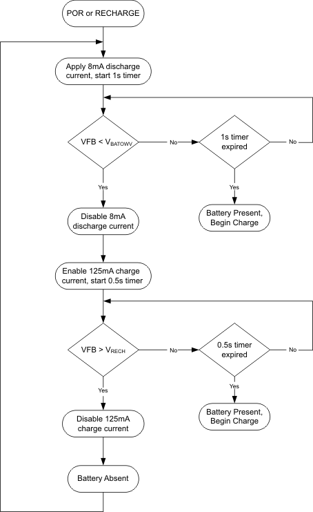 Figure 15. Battery Detection Flow Chart
Once the device has powered up, an 8-mA discharge current is applied to the SRN terminal. If the battery voltage falls below the LOWV threshold within 1 second, the discharge source is turned off, and the charger is turned on at low charge current (125 mA). If the battery voltage gets up above the recharge threshold within 500 ms, there is no battery present and the cycle restarts. If either the 500-ms or 1-second timer times out before the respective thresholds are hit, a battery is detected and a charge cycle is initiated.
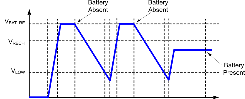 Figure 16. Battery Detect Timing Diagram
Ensure that the total output capacitance at the battery node is not so large that the discharge current source cannot pull the voltage below the LOWV threshold during the 1 second discharge time. The maximum output capacitances can be calculated according to the following equations:


where
- CMAX is the maximum output capacitance.
- IDISCH is the discharge current.
- tDISCH is the discharge time.
- R2 and R1 are the voltage feedback resistors from the battery to the FB pin.
9.3.15.1 Example
For a 3-cell Li+ charger, with R2 = 500 kΩ, R1 = 100 kΩ (giving 12.6 V for voltage regulation), IDISCH = 8 mA, tDISCH = 1 second.

Based on these calculations, no more than 2200 µF should be allowed on the battery node for proper operation of the battery detection circuit.
9.3.16 Battery Short Protection
When SRN pin voltage is lower than 2 V, it is considered as battery short condition during charging period. The charger will shut down immediately for 1 ms, then soft start back to the charging current the same as precharge current. This prevents high current may build in output inductor and cause inductor saturation when battery terminal is shorted during charging. The converter works in nonsynchronous mode during battery short.
9.3.17 Battery Overvoltage Protection
The converter will not allow the high-side FET to turn on until the battery voltage goes below 102% of the regulation voltage. This allows 1-cycle response to an overvoltage condition – such as occurs when the load is removed or the battery is disconnected. A total 6-mA current sink from SRP/SRN to AGND allows discharging the stored output inductor energy that is transferred to the output capacitors. If battery overvoltage condition lasts for more than 30 ms, charge is disabled.
9.3.18 Temperature Qualification
The controller continuously monitors battery temperature by measuring the voltage between the TS pin and AGND. A negative temperature coefficient thermistor (NTC) and an external voltage divider typically develop this voltage. The controller compares this voltage against its internal thresholds to determine if charging is allowed. To initiate a charge cycle, the battery temperature must be within the VLTF to VHTF thresholds. If battery temperature is outside of this range, the controller suspends charge and waits until the battery temperature is within the VLTF to VHTF range. During the charge cycle the battery temperature must be within the VLTF to VTCO thresholds. If battery temperature is outside of this range, the controller suspends charge and waits until the battery temperature is within the VLTF to VHTF range. The controller suspends charge by turning off the PWM charge MOSFETss. Figure 17 summarizes the operation.
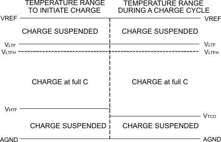 Figure 17. TS Pin, Thermistor Sense Thresholds
Assuming a 103AT NTC thermistor on the battery pack as shown in Figure 18, the values of RT1 and RT2 can be determined by using Equation 10 and Equation 11:


Select 0°C to 45°C range for Li-ion or Li-polymer battery,
RTHCOLD = 27.28 kΩ
RTHHOT = 4.911 kΩ
RT1 = 5.23 kΩ
RT2 = 30.1 kΩ
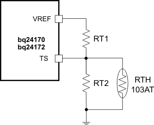 Figure 18. TS Resistor Network
9.3.19 MOSFET Short Circuit and Inductor Short Circuit Protection
The IC has a short circuit protection feature. Its cycle-by-cycle current monitoring feature is achieved through monitoring the voltage drop across Rdson of the MOSFETs. The charger will be latched off, but the ACFET keep on to power the system. The only way to reset the charger from latch-off status is remove adapter then plug adapter in again. Meanwhile, STAT is blinking to report the fault condition.
9.3.20 Thermal Regulation and Shutdown Protection
The QFN package has low thermal impedance, which provides good thermal conduction from the silicon to the ambient, to keep junctions temperatures low. The internal thermal regulation loop will fold back the charge current to keep the junction temperature from exceeding 120°C. As added level of protection, the charger converter turns off and self-protects whenever the junction temperature exceeds the TSHUT threshold of 150°C. The charger stays off until the junction temperature falls below 130°C.
9.3.21 Timer Fault Recovery
The IC provides a recovery method to deal with timer fault conditions. The following summarizes this method:
Condition 1: The battery voltage is above the recharge threshold and a time-out fault occurs.
Recovery Method: The timer fault will clear when the battery voltage falls below the recharge threshold, and battery detection will begin. A POR or taking ISET below 40 mV will also clear the fault.
Condition 2: The battery voltage is below the recharge threshold and a time-out fault occurs.
Recovery Method: Under this scenario, the IC applies the fault current to the battery. This small current is used to detect a battery removal condition and remains on as long as the battery voltage stays below the recharge threshold. If the battery voltage goes above the recharge threshold, the IC disabled the fault current and executes the recovery method described in Condition 1. A POR or taking ISET below 40 mV will also clear the fault.
9.3.22 Inductor, Capacitor, and Sense Resistor Selection Guidelines
The IC provides internal loop compensation. With this scheme, the best stability occurs when the LC resonant frequency, fo, is approximately 15 kHz to 25 kHz for the IC.

Table 3 summarizes typical LC components for various charge currents.
Table 3. Typical Values as a Function of Charge Current
| CHARGE CURRENT | 1 A | 2 A | 3 A | 4 A |
|---|---|---|---|---|
| Output inductor L | 6.8 µH | 3.3 µH | 3.3 µH | 2.2 µH |
| Output capacitor C | 10 µF | 20 µF | 20 µF | 30 µF |
9.3.23 Charge Status Outputs
The open-drain STAT outputs indicate various charger operations as listed in Table 4. These status pins can be used to drive LEDs or communicate with the host processor. OFF indicates that the open-drain transistor is turned off.
Table 4. STAT Pin Definition
| CHARGE STATE | STAT |
|---|---|
| Charge in progress (including recharging) | ON |
| Charge complete, Sleep mode, Charge disabled | OFF |
| Charge suspend, Input overvoltage, Battery overvoltage, timer fault, , battery absent | BLINK |
9.4 Device Functional Modes
The bq2417x is a stand-alone switched-mode charger with power path selector. The device can operate from either a qualified adapter or supply system power from the battery. Dynamic Power Management (DPM) mode allows for a smaller adapter to be used effectively in systems with more dynamic system loads.
The bq2417x device provides power path selector gate driver ACDRV/CMSRC on input NMOS pair ACFET (Q1) and RBFET (Q2), and BATDRV on a battery PMOS device (Q3). When the qualified adapter is present, the system is directly connected to the adapter. Otherwise, the system is connected to the battery. In addition, the power path prevents battery from boosting back to the input.
The bq2417x features DPM to reduce the charge current when the input power limit is reached to avoid overloading the adapter. A highly accurate current-sense amplifier enables precise measurement of input current from adapter to monitor overall system power.
The total input current from an AC adapter or other DC sources is a function of the system supply current and the battery charging current. System current normally fluctuated as portions of the systems are powered up or down. Without DPM, the source must be able to supply the maximum system current and the maximum available charger input current simultaneously. By using DPM, the input current regulator reduces the charging current when the summation of system power and charge power exceeds the maximum input power. Therefore, the current capability of the AC adapter can be lowered, thus reducing system cost.
Although the bq2417x is a stand-alone charger, external control circuitry can effectively be used to change pin settings such as ISET, ACSET, and enable Battery Learn mode to accommodated for dynamic charging conditions.