SLUSAW5B January 2012 – December 2014
PRODUCTION DATA.
- 1 Features
- 2 Applications
- 3 Description
- 4 Revision History
- 5 Description (Continued)
- 6 Device Comparison Table
- 7 Pin Configuration and Functions
- 8 Specifications
-
9 Detailed Description
- 9.1 Overview
- 9.2 Functional Block Diagram
- 9.3
Feature Description
- 9.3.1
Device Power Up
- 9.3.1.1 Power-On-Reset (POR)
- 9.3.1.2 Power Up from Battery without DC Source
- 9.3.1.3
Power Up from DC Source
- 9.3.1.3.1 REGN LDO
- 9.3.1.3.2 Input Source Qualification
- 9.3.1.3.3 Input Current Limit Detection
- 9.3.1.3.4 D+/D- Detection Sets Input Current Limit in bq24190
- 9.3.1.3.5 PSEL/OTG Pins Set Input Current Limit in bq24192, bq24192I
- 9.3.1.3.6 HIZ State wth 100mA USB Host
- 9.3.1.3.7 Force Input Current Limit Detection
- 9.3.1.4 Converter Power-Up
- 9.3.1.5 Boost Mode Operation from Battery
- 9.3.2 Power Path Management
- 9.3.3 Battery Charging Management
- 9.3.4 Status Outputs (PG, STAT, and INT)
- 9.3.5 Protections
- 9.3.6 Serial Interface
- 9.3.1
Device Power Up
- 9.4 Device Functional Modes
- 9.5
Register Map
- 9.5.1
I2C Registers
- 9.5.1.1 Input Source Control Register REG00 (bq24190, bq24192 reset = 00110000, or 30; bq24192I reset = 00111000, or 38)
- 9.5.1.2 Power-On Configuration Register REG01 (reset = 00011011, or 1B)
- 9.5.1.3 Charge Current Control Register REG02 (bq24190, bq24192 reset = 01100000, or 60; bq24192I reset = 00100000, or 20)
- 9.5.1.4 Pre-Charge/Termination Current Control Register REG03 (reset = 00010001, or 11)
- 9.5.1.5 Charge Voltage Control Register REG04 (bq24190, bq241192 reset = 10110010, or B2; bq24192I reset = 10011010, or 9A)
- 9.5.1.6 Charge Termination/Timer Control Register REG05 (reset = 10011010, or 9A)
- 9.5.1.7 IR Compensation / Thermal Regulation Control Register REG06 (reset = 00000011, or 03)
- 9.5.1.8 Misc Operation Control Register REG07 (reset = 01001011, or 4B)
- 9.5.1.9 System Status Register REG08
- 9.5.1.10 Fault Register REG09
- 9.5.1.11 Vender / Part / Revision Status Register REG0A (bq24190 reset = 00100011, or 23; bq24192 reset = 00101011, or 2B; bq24192I reset = 00001011, or 0B)
- 9.5.1
I2C Registers
- 10Application and Implementation
- 11Power Supply Recommendations
- 12Layout
- 13Device and Documentation Support
- 14Mechanical, Packaging, and Orderable Information
Package Options
Mechanical Data (Package|Pins)
- RGE|24
Thermal pad, mechanical data (Package|Pins)
- RGE|24
Orderable Information
12 Layout
12.1 Layout Guidelines
The switching node rise and fall times should be minimized for minimum switching loss. Proper layout of the components to minimize high frequency current path loop (see Figure 51) is important to prevent electrical and magnetic field radiation and high frequency resonant problems. Here is a PCB layout priority list for proper layout. Layout PCB according to this specific order is essential.
- Place input capacitor as close as possible to PMID pin and GND pin connections and use shortest copper trace connection or GND plane.
- Place inductor input terminal to SW pin as close as possible. Minimize the copper area of this trace to lower electrical and magnetic field radiation but make the trace wide enough to carry the charging current. Do not use multiple layers in parallel for this connection. Minimize parasitic capacitance from this area to any other trace or plane.
- Put output capacitor near to the inductor and the IC. Ground connections need to be tied to the IC ground with a short copper trace connection or GND plane.
- Route analog ground separately from power ground. Connect analog ground and connect power ground separately. Connect analog ground and power ground together using power pad as the single ground connection point. Or using a 0-Ω resistor to tie analog ground to power ground.
- Use single ground connection to tie charger power ground to charger analog ground. Just beneath the IC. Use ground copper pour but avoid power pins to reduce inductive and capacitive noise coupling.
- Decoupling capacitors should be placed next to the IC pins and make trace connection as short as possible.
- It is critical that the exposed power pad on the backside of the IC package be soldered to the PCB ground. Ensure that there are sufficient thermal vias directly under the IC, connecting to the ground plane on the other layers.
- The via size and number should be enough for a given current path.
See the EVM design for the recommended component placement with trace and via locations. For the VQFN information, refer to SCBA017 and SLUA271.
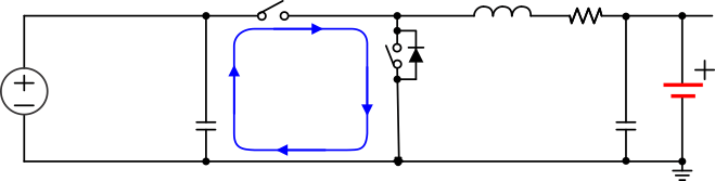 Figure 51. High Frequency Current Path
12.2 Layout Example
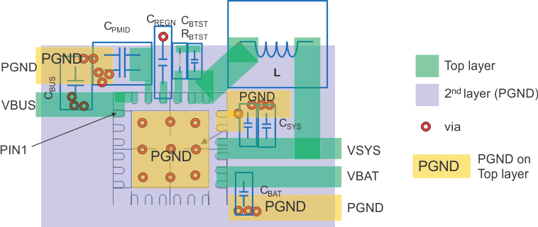 Figure 52. Layout Example Diagram