SLUSA76B December 2010 – January 2015
PRODUCTION DATA.
- 1 Features
- 2 Applications
- 3 Description
- 4 Typical Application Schematic
- 5 Revision History
- 6 Pin Configuration and Functions
- 7 Specifications
-
8 Detailed Description
- 8.1 Overview
- 8.2 Functional Block Diagram
- 8.3 Feature Description
- 8.4
Device Functional Modes
- 8.4.1 Power-Down or Undervoltage Lockout (UVLO)
- 8.4.2 Operation Mode Detection and Transition
- 8.4.3 Sleep Mode
- 8.4.4 Load Mode
- 8.4.5
Charge Mode
- 8.4.5.1 Overvoltage Protection (OVP) - Continuously Monitored
- 8.4.5.2 Power Up
- 8.4.5.3 Battery Detect Routine
- 8.4.5.4 New Charge Cycle
- 8.4.5.5 BAT Output
- 8.4.5.6 Fast Charge Current (IOUT)
- 8.4.5.7 Termination
- 8.4.5.8 Timers
- 8.4.5.9 Battery Temperature Monitoring
- 8.4.5.10 Limited Power Charge Mode - TS Pin High
- 8.4.6 Suspend Mode
- 9 Application and Implementation
- 10Power Supply Recommendations
- 11Layout
- 12Device and Documentation Support
- 13Mechanical, Packaging, and Orderable Information
Package Options
Mechanical Data (Package|Pins)
- DQC|10
Thermal pad, mechanical data (Package|Pins)
- DQC|10
Orderable Information
9 Application and Implementation
NOTE
Information in the following applications sections is not part of the TI component specification, and TI does not warrant its accuracy or completeness. TI’s customers are responsible for determining suitability of components for their purposes. Customers should validate and test their design implementation to confirm system functionality.
9.1 Application Information
Although it can be powered from low impedance sources like a USB port or wall adapter, this IC's VBUS-DPM feature makes it ideal to be powered from high impedance sources like solar panels or inductor charging pads.
9.2 Typical Application

9.2.1 Design Requirements
A solar panel with VOC = 6 V in direct sunlight and capable of up to 1 W of output power is available to charge a 500 mAHr LiIon battery at a 1C rate. Because the light itensity will vary over time, this application uses the IC in battery tracking mode. The IC will never use load mode so EN is tied to PG.
9.2.2 Detailed Design Procedure
The minimum recommend capacitors of 1 µF for VBUS and BAT are used. The pullup resistors for CHG and PG are 2 kΩ.
Using RISET = KISET / IOUT and set IOUT = IC = 500mA gives RISET = 390 AΩ / 500 mA = 780 Ω → 787 Ω closest 1% resistor.
Using Equation 3 and finding RTH(45) from the 103AT-4 thermistor datasheet as 4911 Ω, RT1 = 1 / (0.186) * 4911 Ω - 4911 Ω = 21.492 kΩ → 21.5 kΩ closest 1% resistor.
For battery tracking mode, we leave VDPM floating. If we decided to power the charger using a 5-V wall adapter that a minimum output voltage of 4.6 V, we would size a resistor VDPM to ground using RVDPM = (VBUS_DPM – VBUS_DPM_1)/KVBUS_DPM= (4.6 V - 3.5 V) / ( 0.15 V/kΩ) = 7.333 kΩ → 7.32 kΩ closest 1% resistor.
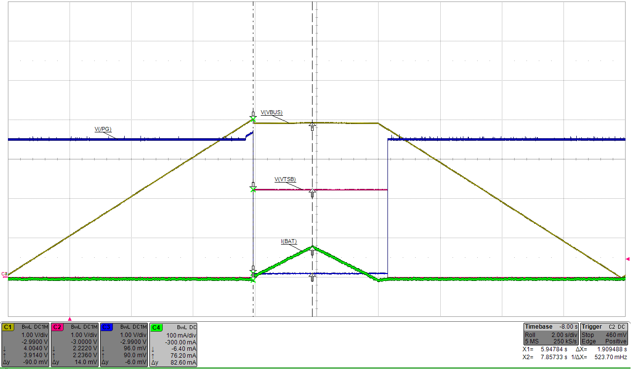
9.2.3 Application Curves