SLUSA76B December 2010 – January 2015
PRODUCTION DATA.
- 1 Features
- 2 Applications
- 3 Description
- 4 Typical Application Schematic
- 5 Revision History
- 6 Pin Configuration and Functions
- 7 Specifications
-
8 Detailed Description
- 8.1 Overview
- 8.2 Functional Block Diagram
- 8.3 Feature Description
- 8.4
Device Functional Modes
- 8.4.1 Power-Down or Undervoltage Lockout (UVLO)
- 8.4.2 Operation Mode Detection and Transition
- 8.4.3 Sleep Mode
- 8.4.4 Load Mode
- 8.4.5
Charge Mode
- 8.4.5.1 Overvoltage Protection (OVP) - Continuously Monitored
- 8.4.5.2 Power Up
- 8.4.5.3 Battery Detect Routine
- 8.4.5.4 New Charge Cycle
- 8.4.5.5 BAT Output
- 8.4.5.6 Fast Charge Current (IOUT)
- 8.4.5.7 Termination
- 8.4.5.8 Timers
- 8.4.5.9 Battery Temperature Monitoring
- 8.4.5.10 Limited Power Charge Mode - TS Pin High
- 8.4.6 Suspend Mode
- 9 Application and Implementation
- 10Power Supply Recommendations
- 11Layout
- 12Device and Documentation Support
- 13Mechanical, Packaging, and Orderable Information
Package Options
Mechanical Data (Package|Pins)
- DQC|10
Thermal pad, mechanical data (Package|Pins)
- DQC|10
Orderable Information
11 Layout
11.1 Layout Guidelines
The minimum VBUS and BAT capacitors, CVBUS and CBAT, of 1 uF are required to be placed as close as possible between the respective pins and the IC ground pin. Higher bulk capacitance values and additional high frequency (< 0.1 uF) bypass capacitors are allowed. Next, the resistor on ISET, RISET, and on VDPM, RVDPM, should be placed as close as possible to the respective pins and the IC ground pin. The TS pullup resistor, RVTSB or RT1, can then be placed between the VTSB and TS pins. Optional capacitors up to 1.0 uF on TS, CTS, and VTSB, CVTSB, can be placed to minimize noise coupling.
11.2 Layout Example
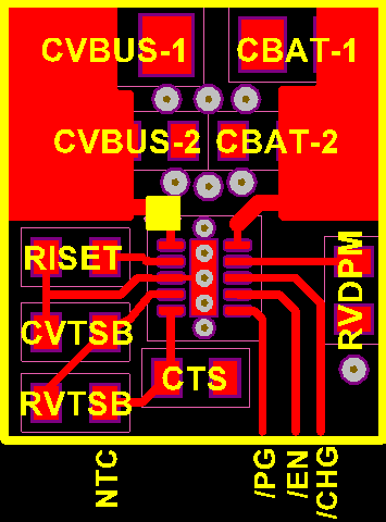 Figure 16. Recommended Layout