SLUS821J October 2008 – May 2017
PRODUCTION DATA.
- 1 Features
- 2 Applications
- 3 Description
- 4 Revision History
- 5 Device Comparison Table
- 6 Pin Configuration and Functions
- 7 Specifications
-
8 Detailed Description
- 8.1 Overview
- 8.2 Functional Block Diagram
- 8.3 Feature Description
- 8.4 Device Functional Modes
-
9 Application and Implementation
- 9.1 Application Information
- 9.2
Typical Applications
- 9.2.1 Using The bq24232 In A Stand-Alone Charger Application
- 9.2.2 Using The bq24230 in a Host Controlled Charger Application
- 10Power Supply Recommendations
- 11Layout
- 12Device and Documentation Support
- 13Mechanical, Packaging, and Orderable Information
Package Options
Mechanical Data (Package|Pins)
- RGT|16
Thermal pad, mechanical data (Package|Pins)
- RGT|16
Orderable Information
7 Specifications
7.1 Absolute Maximum Ratings
over operating free-air temperature range (unless otherwise noted) (1)
(1) Stresses beyond those listed under Absolute Maximum Ratings may cause permanent damage to the device. These are stress ratings only, which do not imply functional operation of the device at these or any other conditions beyond those indicated under Recommended Operating Conditions. Exposure to absolute-maximum-rated conditions for extended periods may affect device reliability. All voltage values are with respect to the network ground terminal unless otherwise noted.
7.2 ESD Ratings
| VALUE | UNIT | ||||
|---|---|---|---|---|---|
| V(ESD) | Electrostatic discharge | Human body model (HBM), per ANSI/ESDA/JEDEC JS-001, all pins(1) | ±1000 | V | |
| Charged device model (CDM), per JEDEC specification JESD22-C101, all pins(2) | ±250 | ||||
(1) JEDEC document JEP155 states that 500-V HBM allows safe manufacturing with a standard ESD control process.
(2) JEDEC document JEP157 states that 250-V CDM allows safe manufacturing with a standard ESD control process.
7.3 Recommended Operating Conditions
over operating free-air temperature range (unless otherwise noted)7.4 Thermal Information
| THERMAL METRIC(1) | bq24230 | bq24232 | UNIT | |
|---|---|---|---|---|
| RGT | RGT | |||
| 16 PINS | 16 PINS | |||
| RθJA | Junction-to-ambient thermal resistance | 44.5 | 44.5 | °C/W |
| RθJC(top) | Junction-to-case (top) thermal resistance | 54.2 | 54.2 | °C/W |
| RθJB | Junction-to-board thermal resistance | 17.2 | 17.2 | °C/W |
| ψJT | Junction-to-top characterization parameter | 1.0 | 1.0 | °C/W |
| ψJB | Junction-to-board characterization parameter | 17.1 | 17.1 | °C/W |
| RθJC(bot) | Junction-to-case (bottom) thermal resistance | 3.8 | 3.8 | °C/W |
(1) For more information about traditional and new thermal metrics, see the IC Package Thermal Metrics application report, SPRA953.
7.5 Electrical Characteristics
over operating free-air temperature range (unless otherwise noted)| PARAMETER | TEST CONDITIONS | MIN | TYP | MAX | UNIT | |
|---|---|---|---|---|---|---|
| INPUT | ||||||
| UVLO | Undervoltage lockout | VIN: 0 V → 4 V | 3.2 | 3.3 | 3.4 | V |
| Vhys(UVLO) | Hysteresis on UVLO | VIN: 4 V → 0 V | 200 | 300 | mV | |
| VIN(DT) | Input power detection threshold | Input power detected when VIN > VBAT + VIN(DT)
VBAT = 3.6 V, VIN: 3.5 V → 4 V |
55 | 80 | 130 | mV |
| Vhys(INDT) | Hysteresis on VIN(DT) | VBAT = 3.6 V, VIN: 4 V → 3.5 V | 20 | mV | ||
| VOVP | Input overvoltage protection threshold | ('230) VIN: 5 V → 7 V | 6.4 | 6.6 | 6.8 | V |
| ('232) VIN: 5 V → 11 V | 10.2 | 10.5 | 10.8 | |||
| Vhys(OVP) | Hysteresis on OVP | ('230) VIN: 7 V → 5V | 110 | mV | ||
| ('232) VIN: 11 V → 5 V | 175 | |||||
| ILIM, TEST ISET SHORT CIRCUIT | ||||||
| ISC | Current source | VIN > UVLO and VIN > VBAT+VIN(DT) | 1.3 | mA | ||
| VSC | VIN > UVLO and VIN > VBAT+VIN(DT) | 520 | mV | |||
| QUIESCENT CURRENT | ||||||
| IBAT(PDWN) | Sleep current into BAT pin | CE = LO or HI, input power not detected, no load on OUT pin, TJ=85°C |
6.5 | μA | ||
| IIN(STDBY) | Standby current into IN pin | EN1= HI, EN2=HI, VIN = 6 V, TJ=85°C | 50 | μA | ||
| EN1= HI, EN2=HI, VIN = 10 V, TJ=85°C | 200 | |||||
| ICC | Active supply current, IN pin | CE = LO, VIN = 6 V, no load on OUT pin, VBAT > VBAT(REG), (EN1, EN2) ≠ (HI, HI) |
1.5 | mA | ||
| POWER PATH | ||||||
| VDO(IN-OUT) | VIN – VOUT | VIN = 4.3 V, IIN = 500 mA, VBAT = 4.2 V | 150.0 | 237.5 | mV | |
| VDO(BAT-OUT) | VBAT – VOUT | IOUT = 500 mA, VIN = 0 V, VBAT > 3 V | 62.5 | mV | ||
| VO(REG) | OUT pin voltage regulation | VIN > VOUT + VDO (IN-OUT) | 4.3 | 4.4 | 4.5 | V |
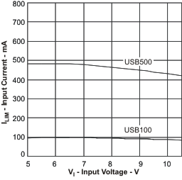
| IINmax | Maximum input current | EN1 = LO, EN2 = LO | 90 | 95 | 100 | mA |
| EN1 = HI, EN2 = LO | 450 | 475 | 500 | |||
| EN2 = HI, EN1 = LO | KILIM/RILIM | A | ||||
| KILIM | Maximum input current factor | ILIM = 200 mA to 500 mA | 1380 | 1530 | 1680 | AΩ |
| IINmax | Programmable input current limit range | EN2 = HI, EN1 = LO, RILIM = 2.75 kΩ to 8.4 kΩ | 200 | 500 | mA | |
| VIN-DPM | Input voltage threshold when input current is reduced | EN2 = LO, EN1 = X | 4.35 | 4.50 | 4.63 | V |
| VDPPM | Output voltage threshold when charging current is reduced | VO(REG) – 180 mV | VO(REG) – 100 mV |
VO(REG) – 30 mV | V | |
| VBSUP1 | Enter battery supplement mode | VBAT = 3.6 V, RILIM = 1.5 kΩ, RLOAD = 10 Ω →2 Ω | VOUT ≤ VBAT –40 mV | V | ||
| VBSUP2 | Exit battery supplement mode | VBAT = 3.6 V, RILIM = 1.5 kΩ, RLOAD = 2 Ω →10 Ω | VOUT ≥ VBAT–20 mV | V | ||
| VO(SC1) | Output short-circuit detection threshold, power-on | VIN > UVLO and VIN > VBAT+VIN(DT) | 0.8 | 0.9 | 1 | V |
| VO(SC2) | Output short-circuit detection threshold, supplement mode VBAT – VOUT > VO(SC2) indicates short circuit | VIN > UVLO and VIN > VBAT+VIN(DT) | 200 | 250 | 300 | mV |
| BATTERY CHARGER | ||||||
| IBAT(SC) | Source current for BAT pin short-circuit detection | VBAT = 1.5 V | 4 | 7.5 | 11 | mA |
| VBAT(SC) | BAT pin short-circuit detection threshold | VBAT rising | 1.6 | 1.8 | 2 | V |
| VBAT(REG) | Battery charge voltage | 4.16 | 4.20 | 4.23 | V | |
| VLOWV | Precharge to fast-charge transition threshold | VIN > UVLO and VIN > VBAT + VIN(DT) | 2.9 | 3 | 3.1 | V |
| ICHG | Battery fast-charge current range | VBAT(REG) > VBAT > VLOWV, VIN = 5 V, CE = LO, EN1 = LO, EN2 = HI | 25 | 500 | mA | |
| Battery fast-charge current | CE = LO, EN1= LO, EN2 = HI, VBAT > VLOWV, VIN = 5 V, IINmax > ICHG, no load on OUT pin, thermal loop and DPM loop not active |
KISET/RISET | A | |||
| KISET | Fast-charge current factor | 25 mA ≥ ICHG≥ 500 mA | 797 | 870 | 975 | AΩ |
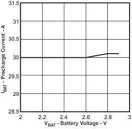
| KIPRECHG | Precharge current factor | 2.5 mA ≥ IPRECHG≥ 30 mA | 70 | 88 | 106 | AΩ |
| ITERM | Termination comparator threshold for termination detection | CE = LO, (EN1,EN2) ≠ (LO,LO), VBAT > VRCH, t < tMAXCH, VIN = 5 V, DPM loop and thermal loop not active |
0.09*ICHG | 0.1*ICHG | 0.11*ICHG | A |
| CE = LO, (EN1,EN2) = (LO,LO), VBAT > VRCH, t < tMAXCH, VIN = 5 V, DPM loop and thermal loop not active |
0.027*ICHG | 0.033*ICHG | 0.040*ICHG | |||
| ITERM | Termination current threshold factor (bq24232) | ITERM = 0% to 50% of ICHG | KITERM*RITERM/RISET | A | ||
| IBIAS(ITERM) | Current for external termination-setting resistor | 72 | 75 | 78 | μA | |
| KITERM | K factor for termination detection threshold (externally set) (bq24232) | CE = LO, (EN1,EN2) ≠ (LO,LO), VBAT > VRCH, t < tMAXCH, VIN = 5 V, DPM loop and thermal loop not active |
0.024 | 0.030 | 0.036 | A |
| CE = LO, (EN1,EN2) = (LO,LO), VBAT > VRCH, t < tMAXCH, VIN = 5 V, DPM loop and thermal loop not active |
0.009 | 0.010 | 0.011 | |||
| IBIAS(ITERM) | Current for external termination_setting resistor (bq24232) | 72 | 75 | 78 | μA | |
| VRCH | Recharge detection threshold | VIN > UVLO and VIN > VBAT+VIN(DT) | VBAT(REG) –140 mV | VBAT(REG) –100 mV | VBAT(REG) –60 mV | V |
| IBAT(DET) | Sink current for battery detection | VBAT=2.5 V | 5 | 7.5 | 10 | mA |
| BATTERY-PACK NTC MONITOR(1) | ||||||
| INTC | NTC bias current | VIN > UVLO and VIN > VBAT+VIN(DT) | 72 | 75 | 78 | μA |
| VHOT | High-temperature trip point | Battery charging, VTS Falling | 270 | 300 | 330 | mV |
| VHYS(HOT) | Hysteresis on high trip point | Battery charging, VTS Rising from VHOT | 30 | mV | ||
| VCOLD | Low-temperature trip point | Battery charging, VTS Rising | 2000 | 2100 | 2200 | mV |
| VHYS(COLD) | Hysteresis on low trip point | Battery charging, VTS Falling from VCOLD | 300 | mV | ||
| VDIS(TS) | TS function disable threshold | TS unconnected | VIN-200 mV | V | ||
| THERMAL REGULATION | ||||||
| TJ(REG) | Temperature regulation limit | 125 | °C | |||
| TJ(OFF) | Thermal shutdown temperature | TJ rising | 155 | °C | ||
| TJ(OFF-HYS) | Thermal shutdown hysteresis | 20 | °C | |||
| LOGIC LEVELS ON EN1, EN2, CE, TD | ||||||
| VIL | Logic LOW input voltage | 0 | 0.4 | V | ||
| VIH | Logic HIGH input voltage | 1.4 | 6.0 | V | ||
| IIL | Input sink current | VIL = 0 V | 1 | μA | ||
| IIH | Input source current | VIH = 1.4 V | 10 | μA | ||
| LOGIC LEVELS ON PGOOD, CHG | ||||||
| VOL | Output LOW voltage | ISINK = 5 mA | 0.4 | V | ||
(1) These numbers set trip points of 0°C and 50°C while charging, with 3°C hysteresis on the trip points, with a Vishay Type 2 curve NTC with an R25 of 10 kΩ.
7.6 Timing Requirements
over operating free-air temperature range (unless otherwise noted)| PARAMETER | TEST CONDITIONS | MIN | TYP | MAX | UNIT | |
|---|---|---|---|---|---|---|
| INPUT | ||||||
| tDGL(PGOOD) | Deglitch time, input power detected status | Time measured from VIN: 0 V → 5-V 1-μs rise time to PGOOD = LO |
2 | ms | ||
| tDGL(OVP) | Input overvoltage blanking time | 50 | μs | |||
| tREC(OVP) | Input overvoltage recovery time | Time measured from VIN: 11 V → 5-V 1-μs fall time to PGOOD = LO |
2 | ms | ||
| POWER PATH | ||||||
| tDGL(SC2) | Deglitch time, supplement mode short circuit | 250 | μs | |||
| tREC(SC2) | Recovery time, supplement mode short circuit | 60 | ms | |||
| BATTERY CHARGER | ||||||
| tDGL1(LOWV) | Deglitch time on precharge to fast-charge transition | 25 | ms | |||
| tDGL2(LOWV) | Deglitch time on fast-charge to precharge transition | 25 | ms | |||
| tDGL(TERM) | Deglitch time, termination detected | 25 | ms | |||
| tDGL(RCH) | Deglitch time, recharge threshold detected | 62.5 | ms | |||
| tDGL(NO-IN) | Delay time, input power loss to charger turnoff | VBAT = 3.6 V. Time measured from VIN: 5 V → 3 V 1-μs fall time |
20 | ms | ||
| BATTERY CHARGING TIMERS | ||||||
| tPRECHG | Precharge safety timer value | TMR = floating | 1440 | 1800 | 2160 | s |
| tMAXCHG | Charge safety timer value | TMR = floating | 14400 | 18000 | 21600 | s |
| tPRECHG | Precharge safety timer value | 18 kΩ < RTMR < 72 kΩ | RTMR × KTMR | s | ||
| tMAXCHG | Charge safety timer value | 18 kΩ < RTMR < 72 kΩ | 10×RTMR ×KTMR | s | ||
| KTMR | Timer factor | 36 | 48 | 60 | s/kΩ | |
| BATTERY-PACK NTC MONITOR(1) | ||||||
| tDGL(TS) | Deglitch time, pack temperature fault detection | Battery charging, VTS Falling | 50 | ms | ||
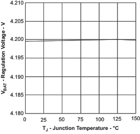
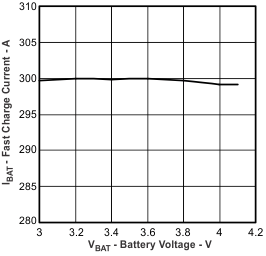
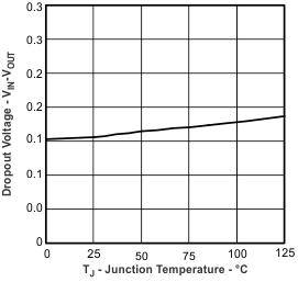
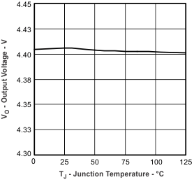
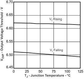
7.7 Typical Characteristics
Typical Application Circuit, EN1=0, EN2=1, TA=25°C, unless otherwise noted.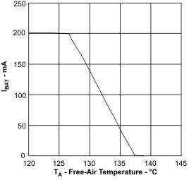
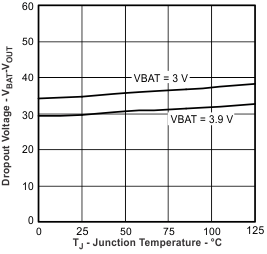
| IL = 500 mA |
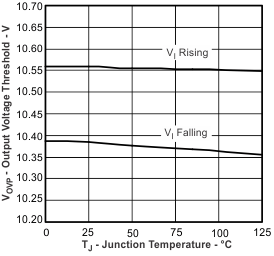
| 10.5 V |
| RISET = 3.3 kΩ |
| IL = 500 mA |
| VIN = 5 V | IL = 500 mA |
| 6.6 V | ||
| RISET = 3.3 kΩ |