SLIS160D August 2014 – March 2017 BQ24392-Q1
PRODUCTION DATA.
- 1 Features
- 2 Applications
- 3 Description
- 4 Revision History
- 5 Pin Configuration and Functions
- 6 Specifications
- 7 Detailed Description
- 8 Application and Implementation
- 9 Power Supply Recommendations
- 10Layout
- 11Device and Documentation Support
- 12Mechanical, Packaging, and Orderable Information
Package Options
Mechanical Data (Package|Pins)
- RSE|10
Thermal pad, mechanical data (Package|Pins)
Orderable Information
6 Specifications
6.1 Absolute Maximum Ratings
over –40℃ to 125℃ temperature range (unless otherwise noted)| MIN | MAX | UNIT | ||
|---|---|---|---|---|
| Input Voltage | VBUS | –2 | 28 | V |
| CHG_AL_N | –2 | 28 | ||
| DM_HOST | –0.3 | 7 | ||
| DP_HOST | –0.3 | 7 | ||
| GOOD_BAT | –0.3 | 7 | ||
| DP_CON | –0.3 | 7 | ||
| DM_CON | –0.3 | 7 | ||
| CHG_DET | –0.3 | 7 | ||
| Tstg | Storage temperature range | –65 | 150 | °C |
6.2 ESD Ratings
| VALUE | UNIT | ||||
|---|---|---|---|---|---|
| V(ESD) | Electrostatic discharge | Human body model (HBM), per AEC Q100-002(1) | ±4000 | V | |
| Charged device model (CDM), per AEC Q100-011 | Corner pins (DP_CON and DM_CON to GND) | ±8000 | |||
| Other pins | ±1500 | ||||
(1) AEC Q100-002 indicates HBM stressing is done in accordance with the ANSI/ESDA/JEDEC JS-001 specification.
6.3 Recommended Operating Conditions
| MIN | MAX | UNIT | ||
|---|---|---|---|---|
| VBUS | 4.75 | 5.25 | V | |
| GOOD_BAT | 0 | VBUS | ||
| DM_HOST | 0 | 3.6 | ||
| DP_HOST | 0 | 3.6 | ||
| DM_CON | 0 | 3.6 | ||
| DP_CON | 0 | 3.6 | ||
6.4 Thermal Information
| THERMAL METRIC(1) | BQ24392-Q1 | UNIT | |
|---|---|---|---|
| RSE | |||
| 10 PINS | |||
| RθJA | Junction-to-ambient thermal resistance | 167.7 | °C/W |
| RθJC(top) | Junction-to-case (top) thermal resistance | 78.8 | °C/W |
| RθJB | Junction-to-board thermal resistance | 95.8 | °C/W |
| ψJT | Junction-to-top characterization parameter | 4.7 | °C/W |
| ψJB | Junction-to-board characterization parameter | 95.9 | v |
(1) For more information about traditional and new thermal metrics, see the Semiconductor and IC Package Thermal Metrics application report.
6.5 Electrical Characteristics
VBUS = 4.5 V to 5.5 V, TA = –40°C to 125°C (unless otherwise noted)| PARAMETER | TEST CONDITIONS | MIN | TYP | MAX | UNIT | ||
|---|---|---|---|---|---|---|---|
| VBUS_VALID | VBUS Valid threshold | Rising VBUS threshold | 3.5 | V | |||
| VOH | CHG_DET | CHG_DET | IOH = –2 mA | 3.5 | VBUS(1) | V | |
| VOL | CHG_DET, SW_OPEN, CHG_AL_N | CHG_DET, SW_OPEN, CHG_AL_N | IOL = 2 mA | 0.4 | V | ||
| VIH | High-level input voltage | GOOD_BAT | 1.1 | V | |||
| VIL | Low-level input voltage | 0.5 | V | ||||
| RPD | Internal pull-down resistance | 950 | kΩ | ||||
| tDBP | Dead battery provision timer | 32 | 45 | Mins | |||
| VUSBIO | Analog signal range | DM_CON, DP_CON, DM_HOST, DP_HOST | 0 | 3.6 | V | ||
| RON | ON-state resistance | VDM_HOST and VDP_HOST = 0 to 3.6 V, IDP_CON and IDM_CON = –2 mA | 6 | 8 | Ω | ||
| RON(flat) | ON-state resistance flatness | 1.1 | 2.4 | Ω | |||
| ΔRON | ON- state resistance match between channels | VDM_HOST and VDP_HOST = 0.4 V, IDP_CON and IDM_CON = –2 mA | 0.5 | Ω | |||
| ICC-SW (ON) | Current consumption | VVBUS = 5 V, USB Switch ON; VIH(GOOD_BAT)= 1.1 V |
250 | 350 | µA | ||
| VVBUS = 5 V, USB Switch ON; VIH(GOOD_BAT) = 2.5 V |
80 | 115 | µA | ||||
| ICC-SW (OFF) | Current consumption with USB switch off | VVBUS = 5 V; USB Switch OFF | 45 | 75 | µA | ||
| IUSBI/O (ON) | Output port leakage current with USB switch on | VI = OPEN, VO = 0.3 V or 2.7 V, Switch ON | 50 | 90 | nA | ||
| IUSBI/O (OFF) | Leakage current with USB switch off | VI = 0.3 V, VO = 2.7 V or VI = 2.7 V, VO = 0.3 V, Switch OFF | 45 | 75 | nA | ||
| CI(OFF) | Capacitance with USB switch off | DP_HOST, DM_HOST | DC bias = 0 V or 3.6 V, f = 10 MHz, Switch OFF | 2 | pF | ||
| CO(OFF) | Capacitance with USB switch off | DP_CON, DM_CON | 10 | pF | |||
| CI(ON) | Capacitance with USB switch on | DP_HOST, DM_HOST | DC bias = 0 V or 3.6 V, f = 10 MHz, Switch ON | 11 | pF | ||
| CO(ON) | Capacitance with USB switch on | DP_CON, DM_CON | 11 | pF | |||
| BW | Bandwidth | RL = 50 Ω, Switch ON | 1 | GHz | |||
| OISO | Isolation with USB switch off | f = 240 MHz, RL = 50 Ω, Switch OFF | –26 | dB | |||
| XTALK | Crosstalk | f = 240 MHz, RL = 50 Ω | –30.5 | dB | |||
(1) CHG_DET max value will be clamped at 7 V when VVBUS > 7 V
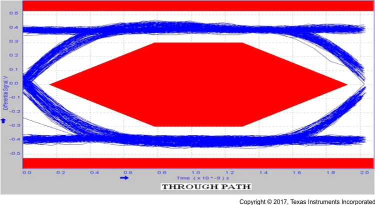
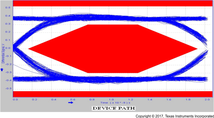
6.6 Typical Characteristics

