SLUSAL0C September 2011 – January 2020 BQ24725A
PRODUCTION DATA.
- 1 Features
- 2 Applications
- 3 Description
- 4 Revision History
- 5 Pin Configuration and Functions
- 6 Specifications
- 7 Parameter Measurement Information
-
8 Detailed Description
- 8.1 Overview
- 8.2 Functional Block Diagram
- 8.3 Feature Description
- 8.4
Device Functional Modes
- 8.4.1 Adapter Detect and ACOK Output
- 8.4.2 Adapter Over Voltage (ACOVP)
- 8.4.3 System Power Selection
- 8.4.4 Battery LEARN Cycle
- 8.4.5 Enable and Disable Charging
- 8.4.6 Automatic Internal Soft-Start Charger Current
- 8.4.7 High Accuracy Current Sense Amplifier
- 8.4.8 Charge Timeout
- 8.4.9 Converter Operation
- 8.4.10 Continuous Conduction Mode (CCM)
- 8.4.11 Discontinuous Conduction Mode (DCM)
- 8.4.12 Input Over Current Protection (ACOC)
- 8.4.13 Charge Over Current Protection (CHGOCP)
- 8.4.14 Battery Over Voltage Protection (BATOVP)
- 8.4.15 Battery Shorted to Ground (BATLOWV)
- 8.4.16 Thermal Shutdown Protection (TSHUT)
- 8.4.17 EMI Switching Frequency Adjust
- 8.4.18 Inductor Short, MOSFET Short Protection
- 8.5 Register Maps
-
9 Application and Implementation
- 9.1 Application Information
- 9.2
Typical Applications
- 9.2.1
Typical System with Two NMOS Selector
- 9.2.1.1 Design Requirements
- 9.2.1.2
Detailed Design Procedure
- 9.2.1.2.1 Negative Output Voltage Protection
- 9.2.1.2.2 Reverse Input Voltage Protection
- 9.2.1.2.3 Reduce Battery Quiescent Current
- 9.2.1.2.4 Inductor Selection
- 9.2.1.2.5 Input Capacitor
- 9.2.1.2.6 Output Capacitor
- 9.2.1.2.7 Power MOSFETs Selection
- 9.2.1.2.8 Input Filter Design
- 9.2.1.2.9 BQ24725A Design Guideline
- 9.2.1.3 Application Curves
- 9.2.2 Simplified System without Power Path
- 9.2.1
Typical System with Two NMOS Selector
- 9.3 System Examples
- 10Power Supply Recommendations
- 11Layout
- 12Device and Documentation Support
- 13Mechanical, Packaging, and Orderable Information
Package Options
Mechanical Data (Package|Pins)
- RGR|20
Thermal pad, mechanical data (Package|Pins)
- RGR|20
Orderable Information
9.2.1.2.8 Input Filter Design
During adapter hot plug-in, the parasitic inductance and input capacitor from the adapter cable form a second order system. The voltage spike at VCC pin maybe beyond IC maximum voltage rating and damage IC. The input filter must be carefully designed and tested to prevent over voltage event on VCC pin.
There are several methods to damping or limit the over voltage spike during adapter hot plug-in. An electrolytic capacitor with high ESR as an input capacitor can damp the over voltage spike well below the IC maximum pin voltage rating. A high current capability TVS Zener diode can also limit the over voltage level to an IC safe level. However these two solutions may not have low cost or small size.
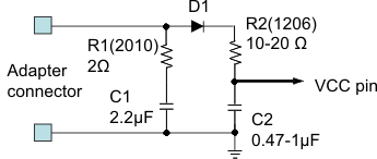
A cost effective and small size solution is shown in Figure 19. The R1 and C1 are composed of a damping RC network to damp the hot plug-in oscillation. As a result the over voltage spike is limited to a safe level. D1 is used for reverse voltage protection for VCC pin. C2 is VCC pin decoupling capacitor and it should be place to VCC pin as close as possible. C2 value should be less than C1 value so R1 can dominant the equivalent ESR value to get enough damping effect. R2 is used to limit inrush current of D1 to prevent D1 getting damage when adapter hot plug-in. R2 and C2 should have 10us time constant to limit the dv/dt on VCC pin to reduce inrush current when adapter hot plug in. R1 has high inrush current. R1 package must be sized enough to handle inrush current power loss according to resistor manufacturer’s datasheet. The filter components value always need to be verified with real application and minor adjustments may need to fit in the real application circuit.
 Figure 19. Input Filter