SLUSDC7A March   2020  – November 2020 BQ25306

PRODUCTION DATA  

  1. Features
  2. Applications
  3. Description
  4. Revision History
  5. Description (continued)
  6. Device Comparison Table
  7. Pin Configuration and Functions
  8. Specifications
    1. 8.1 Absolute Maximum Ratings
    2. 8.2 ESD Ratings
    3. 8.3 Recommended Operating Conditions
    4. 8.4 Thermal Information
    5. 8.5 Electrical Characteristics
    6. 8.6 Timing Requirements
    7. 8.7 Typical Characteristics
  9. Detailed Description
    1. 9.1 Overview
    2. 9.2 Functional Block Diagram
    3. 9.3 Feature Description
      1. 9.3.1 Device Power Up
        1. 9.3.1.1 Power-On-Reset (POR)
        2. 9.3.1.2 REGN Regulator Power Up
        3. 9.3.1.3 Charger Power Up
        4. 9.3.1.4 Charger Enable and Disable by EN Pin
        5. 9.3.1.5 Device Unplugged from Input Source
      2. 9.3.2 Battery Charging Management
        1. 9.3.2.1 Battery Charging Profile
        2. 9.3.2.2 Precharge
        3. 9.3.2.3 Charging Termination
        4. 9.3.2.4 Battery Recharge
        5. 9.3.2.5 Charging Safety Timer
        6. 9.3.2.6 Thermistor Temperature Monitoring
      3. 9.3.3 Charging Status Indicator (STAT)
      4. 9.3.4 Protections
        1. 9.3.4.1 Voltage and Current Monitoring
          1. 9.3.4.1.1 Input Over-Voltage Protection
          2. 9.3.4.1.2 Input Voltage Dynamic Power Management (VINDPM)
          3. 9.3.4.1.3 Input Current Limit
          4. 9.3.4.1.4 Cycle-by-Cycle Current Limit
        2. 9.3.4.2 Thermal Regulation and Thermal Shutdown
        3. 9.3.4.3 Battery Protection
          1. 9.3.4.3.1 Battery Over-Voltage Protection (VBAT_OVP)
          2. 9.3.4.3.2 Battery Short Circuit Protection
        4. 9.3.4.4 ICHG Pin Open and Short Protection
    4. 9.4 Device Functional Modes
      1. 9.4.1 Disable Mode, HiZ Mode, Sleep Mode, Charge Mode, Termination Mode, and Fault Mode
  10. 10Application and Implementation
    1. 10.1 Application Information
    2. 10.2 Typical Applications
      1. 10.2.1 Typical Application
        1. 10.2.1.1 Design Requirements
        2. 10.2.1.2 Detailed Design Procedure
          1. 10.2.1.2.1 Charge Voltage Settings
          2. 10.2.1.2.2 Charge Current Setting
          3. 10.2.1.2.3 Inductor Selection
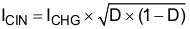
          4. 10.2.1.2.4 Input Capacitor
          5. 10.2.1.2.5 Output Capacitor
        3. 10.2.1.3 Application Curves
      2. 10.2.2 Typical Application with External Power Path
        1. 10.2.2.1 Design Requirements
      3. 10.2.3 Typical Application with MCU Programmable Charge Current
        1. 10.2.3.1 Design Requirements
  11. 11Power Supply Recommendations
  12. 12Layout
    1. 12.1 Layout Guidelines
    2. 12.2 Layout Example
  13. 13Device and Documentation Support
    1. 13.1 Device Support
      1. 13.1.1 Third-Party Products Disclaimer
    2. 13.2 Documentation Support
      1. 13.2.1 Related Documentation
    3. 13.3 Receiving Notification of Documentation Updates
    4. 13.4 Support Resources
    5. 13.5 Trademarks
    6. 13.6 Electrostatic Discharge Caution
    7. 13.7 Glossary
  14. 14Mechanical, Packaging, and Orderable Information

Package Options

Mechanical Data (Package|Pins)
Thermal pad, mechanical data (Package|Pins)
Orderable Information
Input Capacitor

Design input capacitance to provide enough ripple current rating to absorb the input switching ripple current. Worst case RMS ripple current is half of the charging current when the duty cycle is 0.5. If the converter does not operate at 50% duty cycle, then the worst case capacitor RMS current ICin occurs where the duty cycle is closest to 50% and can be estimated using Equation 5.

Equation 5. GUID-129D9564-4889-4252-8787-3E2091DDD447-low.gif

A low ESR ceramic capacitor such as X7R or X5R is preferred for the input decoupling capacitor and should be placed as close as possible to the drain of the high-side MOSFET and source of the low-side MOSFET. The voltage rating of the capacitor must be higher than the normal input voltage level. A rating of 25-V or higher capacitor is preferred for 15-V input voltage.