SLUSDA2B July   2018  ā€“ February 2022 BQ25601D

PRODUCTION DATA  

  1. Features
  2. Applications
  3. Description
  4. Revision History
  5. Description (continued)
  6. Device Comparison Table
  7. Pin Configuration and Functions
  8. Specifications
    1. 8.1 Absolute Maximum Ratings
    2. 8.2 ESD Ratings
    3. 8.3 Recommended Operating Conditions
    4. 8.4 Thermal information
    5. 8.5 Electrical Characteristics
    6. 8.6 Timing Requirements
    7. 8.7 Typical Characteristics
  9. Detailed Description
    1. 9.1 Overview
    2. 9.2 Functional Block Diagram
    3. 9.3 Feature Description
      1. 9.3.1 Power-On-Reset (POR)
      2. 9.3.2 Device Power Up from Battery without Input Source
      3. 9.3.3 Power Up from Input Source
        1. 9.3.3.1 Power Up REGN Regulation
        2. 9.3.3.2 Poor Source Qualification
        3. 9.3.3.3 Input Source Type Detection
          1. 9.3.3.3.1 D+/Dā€“ Detection Sets Input Current Limit in BQ25601D
        4. 9.3.3.4 Input Voltage Limit Threshold Setting (VINDPM Threshold)
        5. 9.3.3.5 Converter Power-Up
      4. 9.3.4 Boost Mode Operation From Battery
      5. 9.3.5 Host Mode and Standalone Power Management
        1. 9.3.5.1 Host Mode and Default Mode in BQ25601D
      6. 9.3.6 Power Path Management
      7. 9.3.7 Battery Charging Management
        1. 9.3.7.1 Autonomous Charging Cycle
        2. 9.3.7.2 Battery Charging Profile
        3. 9.3.7.3 Charging Termination
        4. 9.3.7.4 Thermistor Qualification
        5. 9.3.7.5 JEITA Guideline Compliance During Charging Mode
        6. 9.3.7.6 Boost Mode Thermistor Monitor During Battery Discharge Mode
        7. 9.3.7.7 Charging Safety Timer
    4. 9.4 Device Functional Modes
      1. 9.4.1 Narrow VDC Architecture
      2. 9.4.2 Dynamic Power Management
      3. 9.4.3 Supplement Mode
      4. 9.4.4 Shipping Mode and QON Pin
        1. 9.4.4.1 BATFET Disable Mode (Shipping Mode)
        2. 9.4.4.2 BATFET Enable (Exit Shipping Mode)
        3. 9.4.4.3 BATFET Full System Reset
        4. 9.4.4.4 QON Pin Operations
      5. 9.4.5 Status Outputs ( PG, STAT, INT )
        1. 9.4.5.1 Power Good Indicator ( PGPin PG_STAT Bit)
        2. 9.4.5.2 Charging Status indicator (STAT)
        3. 9.4.5.3 Interrupt to Host ( INT)
    5. 9.5 Protections
      1. 9.5.1 Voltage and Current Monitoring in Converter Operation
        1. 9.5.1.1 Voltage and Current Monitoring in Buck Mode
          1. 9.5.1.1.1 Input Overvoltage (ACOV)
          2. 9.5.1.1.2 System Overvoltage Protection (SYSOVP)
      2. 9.5.2 Voltage and Current Monitoring in Boost Mode
        1. 9.5.2.1 VBUS Soft Start
        2. 9.5.2.2 VBUS Output Protection
        3. 9.5.2.3 Boost Mode Overvoltage Protection
      3. 9.5.3 Thermal Regulation and Thermal Shutdown
        1. 9.5.3.1 Thermal Protection in Buck Mode
        2. 9.5.3.2 Thermal Protection in Boost Mode
      4. 9.5.4 Battery Protection
        1. 9.5.4.1 Battery Overvoltage Protection (BATOVP)
        2. 9.5.4.2 Battery Over-Discharge Protection
        3. 9.5.4.3 System Over-Current Protection
    6. 9.6 Programming
      1. 9.6.1 Serial Interface
        1. 9.6.1.1 Data Validity
        2. 9.6.1.2 START and STOP Conditions
        3. 9.6.1.3 Byte Format
        4. 9.6.1.4 Acknowledge (ACK) and Not Acknowledge (NACK)
        5. 9.6.1.5 Slave Address and Data Direction Bit
        6. 9.6.1.6 Single Read and Write
        7. 9.6.1.7 Multi-Read and Multi-Write
    7. 9.7 Register Maps
      1. 9.7.1  REG00 (address = 00) [reset = 00010111]
      2. 9.7.2  REG01 (address = 01) [reset = 00011010]
      3. 9.7.3  REG02 (address = 02) [reset = 10100 010]
      4. 9.7.4  REG03 (address = 03) [reset = 001 0001 0]
      5. 9.7.5  REG04 (address = 04) [reset = 01011000]
      6. 9.7.6  REG05 (address = 05) [reset = 10011111]
      7. 9.7.7  REG06 (address = 06) [reset = 01100110]
      8. 9.7.8  REG07 (address = 07) [reset = 01001100]
      9. 9.7.9  REG08 (address = 08) [reset = xxxxxxxx]
      10. 9.7.10 REG09 (address = 09) [reset = xxxxxxxx]
      11. 9.7.11 REG0A (address = 0A) [reset = xxxxxx00]
      12. 9.7.12 REG0B (address = 0B) [reset = 00111xxx]
  10. 10Layout
    1. 10.1 Layout Guidelines
    2. 10.2 Layout Example
  11. 11Device and Documentation Support
    1. 11.1 Device Support
      1. 11.1.1 Third-Party Products Disclaimer
    2. 11.2 Documentation Support
      1. 11.2.1 Related Documentation
    3. 11.3 Receiving Notification of Documentation Updates
    4. 11.4 Support Resources
    5. 11.5 Trademarks
    6. 11.6 Electrostatic Discharge Caution
    7. 11.7 Glossary

Package Options

Mechanical Data (Package|Pins)
Thermal pad, mechanical data (Package|Pins)
Orderable Information

Narrow VDC Architecture

The device deploys Narrow VDC architecture (NVDC) with BATFET separating system from battery. The minimum system voltage is set by SYS_Min bits. Even with a fully depleted battery, the system is regulated above the minimum system voltage.

When the battery is below minimum system voltage setting, the BATFET operates in linear mode (LDO mode), and the system is typically 180 mV above the minimum system voltage setting. As the battery voltage rises above the minimum system voltage, BATFET is fully on and the voltage difference between the system and battery is the VDS of BATFET.

When the battery charging is disabled and above minimum system voltage setting or charging is terminated, the system is always regulated at typically 50mV above battery voltage. The status register VSYS_STAT bit goes high when the system is in minimum system voltage regulation.
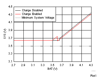
GUID-66B34A91-9A9E-4C8C-8486-F5FAD6C7D109-low.gifFigure 9-7 System Voltage vs Battery Voltage