SLUSCU1A May   2017  – May 2018

PRODUCTION DATA.  

  1. Features
  2. Applications
  3. Description
    1.     Device Images
      1.      Application Diagram
  4. Revision History
  5. Description (continued)
  6. Pin Configuration and Functions
    1.     Pin Functions
  7. Specifications
    1. 7.1 Absolute Maximum Ratings
    2. 7.2 ESD Ratings
    3. 7.3 Recommended Operating Conditions
    4. 7.4 Thermal Information
    5. 7.5 Electrical Characteristics
    6. 7.6 Timing Requirements
    7. 7.7 Typical Characteristics
  8. Detailed Description
    1. 8.1 Overview
    2. 8.2 Functional Block Diagram
    3. 8.3 Feature Description
      1. 8.3.1 Power-Up from Battery Without DC Source
      2. 8.3.2 Power-Up From DC Source
        1. 8.3.2.1 CHRG_OK Indicator
        2. 8.3.2.2 Input Voltage and Current Limit Setup
        3. 8.3.2.3 Battery Cell Configuration
        4. 8.3.2.4 Device Hi-Z State
      3. 8.3.3 USB On-The-Go (OTG)
      4. 8.3.4 Converter Operation
        1. 8.3.4.1 Inductor Setting through IADPT Pin
        2. 8.3.4.2 Continuous Conduction Mode (CCM)
        3. 8.3.4.3 Pulse Frequency Modulation (PFM)
      5. 8.3.5 Current and Power Monitor
        1. 8.3.5.1 High-Accuracy Current Sense Amplifier (IADPT and IBAT)
        2. 8.3.5.2 High-Accuracy Power Sense Amplifier (PSYS)
      6. 8.3.6 Input Source Dynamic Power Manage
      7. 8.3.7 Two-Level Adapter Current Limit (Peak Power Mode)
      8. 8.3.8 Processor Hot Indication
        1. 8.3.8.1 PROCHOT During Low Power Mode
        2. 8.3.8.2 PROCHOT Status
      9. 8.3.9 Device Protection
        1. 8.3.9.1 Watchdog Timer
        2. 8.3.9.2 Input Overvoltage Protection (ACOV)
        3. 8.3.9.3 Input Overcurrent Protection (ACOC)
        4. 8.3.9.4 System Overvoltage Protection (SYSOVP)
        5. 8.3.9.5 Battery Overvoltage Protection (BATOVP)
        6. 8.3.9.6 Battery Short
        7. 8.3.9.7 Thermal Shutdown (TSHUT)
    4. 8.4 Device Functional Modes
      1. 8.4.1 Forward Mode
        1. 8.4.1.1 System Voltage Regulation with Narrow VDC Architecture
        2. 8.4.1.2 Battery Charging
      2. 8.4.2 USB On-The-Go
    5. 8.5 Programming
      1. 8.5.1 I2C Serial Interface
        1. 8.5.1.1 Data Validity
        2. 8.5.1.2 START and STOP Conditions
        3. 8.5.1.3 Byte Format
        4. 8.5.1.4 Acknowledge (ACK) and Not Acknowledge (NACK)
        5. 8.5.1.5 Slave Address and Data Direction Bit
        6. 8.5.1.6 Single Read and Write
        7. 8.5.1.7 Multi-Read and Multi-Write
        8. 8.5.1.8 Write 2-Byte I2C Commands
    6. 8.6 Register Map
      1. 8.6.1  Setting Charge and PROCHOT Options
        1. 8.6.1.1 ChargeOption0 Register (I2C address = 01/00h) [reset = E20Eh]
          1. Table 5. ChargeOption0 Register (I2C address = 01h) Field Descriptions
          2. Table 6. ChargeOption0 Register (I2C address = 00h) Field Descriptions
        2. 8.6.1.2 ChargeOption1 Register (I2C address = 31/30h) [reset = 211h]
          1. Table 7. ChargeOption1 Register (I2C address = 31h) Field Descriptions
          2. Table 8. ChargeOption1 Register (I2C address = 30h) Field Descriptions
        3. 8.6.1.3 ChargeOption2 Register (I2C address = 33/32h) [reset = 2B7]
          1. Table 9.   ChargeOption2 Register (I2C address = 33h) Field Descriptions
          2. Table 10. ChargeOption2 Register (I2C address = 32h) Field Descriptions
        4. 8.6.1.4 ChargeOption3 Register (I2C address = 35/34h) [reset = 0h]
          1. Table 11. ChargeOption3 Register (I2C address = 35h) Field Descriptions
          2. Table 12. ChargeOption3 Register (I2C address = 34h) Field Descriptions
        5. 8.6.1.5 ProchotOption0 Register (I2C address = 37/36h) [reset = 04A54h]
          1. Table 13. ProchotOption0 Register (I2C address = 37h) Field Descriptions
          2. Table 14. ProchotOption0 Register (I2C address = 36h) Field Descriptions
        6. 8.6.1.6 ProchotOption1 Register (I2C address = 39/38h) [reset = 8120h]
          1. Table 15. ProchotOption1 Register (I2C address = 39h) Field Descriptions
          2. Table 16. ProchotOption1 Register (I2C address = 38h) Field Descriptions
        7. 8.6.1.7 ADCOption Register (I2C address = 3B/3Ah) [reset = 2000h]
          1. Table 17. ADCOption Register (I2C address = 3Bh) Field Descriptions
          2. Table 18. ADCOption Register (I2C address = 3Ah) Field Descriptions
      2. 8.6.2  Charge and PROCHOT Status
        1. 8.6.2.1 ChargerStatus Register (I2C address = 21/20h) [reset = 0000h]
          1. Table 19. ChargerStatus Register (I2C address = 21h) Field Descriptions
          2. Table 20. ChargerStatus Register (I2C address = 20h) Field Descriptions
        2. 8.6.2.2 ProchotStatus Register (I2C address = 23/22h) [reset = 0h]
          1. Table 21. ProchotStatus Register (I2C address = 23h) Field Descriptions
          2. Table 22. ProchotStatus Register (I2C address = 22h) Field Descriptions
      3. 8.6.3  ChargeCurrent Register (I2C address = 03/02h) [reset = 0h]
        1. Table 23. Charge Current Register (14h) With 10-mΩ Sense Resistor (I2C address = 03h) Field Descriptions
        2. Table 24. Charge Current Register (14h) With 10-mΩ Sense Resistor (I2C address = 02h) Field Descriptions
        3. 8.6.3.1    Battery Pre-Charge Current Clamp
      4. 8.6.4  MaxChargeVoltage Register (I2C address = 05/04h) [reset value based on CELL_BATPRESZ pin setting]
        1. Table 25. MaxChargeVoltage Register (I2C address = 05h) Field Descriptions
        2. Table 26. MaxChargeVoltage Register (I2C address = 04h) Field Descriptions
      5. 8.6.5  MinSystemVoltage Register (I2C address = 0D/0Ch) [reset value based on CELL_BATPRESZ pin setting]
        1. Table 27. MinSystemVoltage Register (I2C address = 0Dh) Field Descriptions
        2. Table 28. MinSystemVoltage Register (I2C address = 0Ch) Field Descriptions
        3. 8.6.5.1    System Voltage Regulation
      6. 8.6.6  Input Current and Input Voltage Registers for Dynamic Power Management
        1. 8.6.6.1 Input Current Registers
          1. 8.6.6.1.1 IIN_HOST Register With 10-mΩ Sense Resistor (I2C address = 0F/0Eh) [reset = 4000h]
            1. Table 29. IIN_HOST Register With 10-mΩ Sense Resistor (I2C address = 0Fh) Field Descriptions
            2. Table 30. IIN_HOST Register With 10-mΩ Sense Resistor (I2C address = 0Eh) Field Descriptions
          2. 8.6.6.1.2 IIN_DPM Register With 10-mΩ Sense Resistor (I2C address = 25/24h) [reset = 0h]
            1. Table 31. IIN_DPM Register With 10-mΩ Sense Resistor (I2C address = 25h) Field Descriptions
            2. Table 32. IIN_DPM Register With 10-mΩ Sense Resistor (I2C address = 24h) Field Descriptions
          3. 8.6.6.1.3 InputVoltage Register (I2C address = 0B/0Ah) [reset = VBUS-1.28V]
            1. Table 33. InputVoltage Register (I2C address = 0Bh) Field Descriptions
            2. Table 34. InputVoltage Register (I2C address = 0Ah) Field Descriptions
      7. 8.6.7  OTGVoltage Register (I2C address = 07/06h) [reset = 0h]
        1. Table 35. OTGVoltage Register (I2C address = 07h) Field Descriptions
        2. Table 36. OTGVoltage Register (I2C address = 06h) Field Descriptions
      8. 8.6.8  OTGCurrent Register (I2C address = 09/08h) [reset = 0h]
        1. Table 37. OTGCurrent Register (I2C address = 09h) Field Descriptions
        2. Table 38. OTGCurrent Register (I2C address = 08h) Field Descriptions
      9. 8.6.9  ADCVBUS/PSYS Register (I2C address = 27/26h)
        1. Table 39. ADCVBUS/PSYS Register (I2C address = 27h) Field Descriptions
        2. Table 40. ADCVBUS/PSYS Register (I2C address = 26h) Field Descriptions
      10. 8.6.10 ADCIBAT Register (I2C address = 29/28h)
        1. Table 41. ADCIBAT Register (I2C address = 29h) Field Descriptions
        2. Table 42. ADCIBAT Register (I2C address = 28h) Field Descriptions
      11. 8.6.11 ADCIINCMPIN Register (I2C address = 2B/2Ah)
        1. Table 43. ADCIINCMPIN Register (I2C address = 2Bh) Field Descriptions
        2. Table 44. ADCIINCMPIN Register (I2C address = 2Ah) Field Descriptions
      12. 8.6.12 ADCVSYSVBAT Register (I2C address = 2D/2Ch)
        1. Table 45. ADCVSYSVBAT Register (I2C address = 2Dh) Field Descriptions
        2. Table 46. ADCVSYSVBAT Register (I2C address = 2Ch) Field Descriptions
      13. 8.6.13 ID Registers
        1. 8.6.13.1 ManufactureID Register (I2C address = 2Eh) [reset = 0040h]
          1. Table 47. ManufactureID Register Field Descriptions
        2. 8.6.13.2 Device ID (DeviceAddress) Register (I2C address = 2Fh) [reset = 0h]
          1. Table 48. Device ID (DeviceAddress) Register Field Descriptions
  9. Application and Implementation
    1. 9.1 Application Information
    2. 9.2 Typical Application
      1. 9.2.1 Design Requirements
      2. 9.2.2 Detailed Design Procedure
        1. 9.2.2.1 ACP-ACN Input Filter
        2. 9.2.2.2 Inductor Selection
        3. 9.2.2.3 Input Capacitor
        4. 9.2.2.4 Output Capacitor
        5. 9.2.2.5 Power MOSFETs Selection
      3. 9.2.3 Application Curves
  10. 10Power Supply Recommendations
  11. 11Layout
    1. 11.1 Layout Guidelines
    2. 11.2 Layout Example
      1. 11.2.1 Layout Consideration of Current Path
      2. 11.2.2 Layout Consideration of Short Circuit Protection
  12. 12Device and Documentation Support
    1. 12.1 Device Support
      1. 12.1.1 Third-Party Products Disclaimer
    2. 12.2 Documentation Support
      1. 12.2.1 Related Documentation
    3. 12.3 Receiving Notification of Documentation Updates
    4. 12.4 Community Resources
    5. 12.5 Trademarks
    6. 12.6 Electrostatic Discharge Caution
    7. 12.7 Glossary
  13. 13Mechanical, Packaging, and Orderable Information
    1. 13.1 Package Option Addendum
      1. 13.1.1 Packaging Information
      2. 13.1.2 Tape and Reel Information

Package Options

Mechanical Data (Package|Pins)
Thermal pad, mechanical data (Package|Pins)
Orderable Information

Processor Hot Indication

When CPU is running turbo mode, the system peak power may exceed available power from adapter and battery together. The adapter current and battery discharge peak current, or system voltage drop is indication that system power is too high. The charger processor hot function monitors these events, and PROCHOT pulse is asserted. Once CPU receives PROCHOT pulse from charger, it slows down to reduce system power. The processor hot function monitors these events, and PROCHOT pulse is asserted.

The PROCHOT triggering events include:

  • ICRIT: adapter peak current, as 110% of ILIM2
  • INOM: adapter average current (110% of input current limit)
  • IDCHG: battery discharge current
  • VSYS: system voltage on VSYS
  • Adapter Removal: upon adapter removal (CHRG_OK pin HIGH to LOW)
  • Battery Removal: upon battery removal (CELL_BATPRESZ pin goes LOW)
  • CMPOUT: Independent comparator output (CMPOUT pin HIGH to LOW)

The threshold of ICRIT, IDCHG or VSYS, and the deglitch time of ICRIT, INOM, IDCHG or CMPOUT are programmable through I2C. Each triggering event can be individually enabled in REG0x38[6:0]. When any event in PROCHOT profile is triggered, PROCHOT is asserted low for minimum 10 ms programmable in 0x36[4:3]. At the end of the 10 ms, if the PROCHOT event is still active, the pulse gets extended.
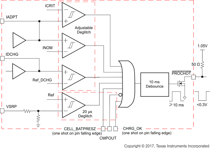
bq25703A prochot_profile_SLUSCU1.gifFigure 13. PROCHOT Profile