SLUSA52C September 2010 – March 2016
PRODUCTION DATA.
- 1 Features
- 2 Applications
- 3 Description
- 4 Revision History
- 5 Device Options
- 6 Pin Configuration and Functions
- 7 Specifications
- 8 Detailed Description
- 9 Application and Implementation
- 10Power Supply Recommendations
- 11Layout
- 12Device and Documentation Support
- 13Mechanical, Packaging, and Orderable Information
Package Options
Refer to the PDF data sheet for device specific package drawings
Mechanical Data (Package|Pins)
- DRB|8
Thermal pad, mechanical data (Package|Pins)
- DRB|8
Orderable Information
1 Features
- 2-Series Cell Secondary Protection
- Automatic Cell Imbalance Correction with External Enable Control
- ±30-mV Enable, 0-mV Disable Thresholds Typical
- External Capacitor-Controlled Delay Timer
- External Resistor-Controlled Cell Balance Current
- Low Power Consumption ICC < 3 µA Typical (VCELL(ALL) < VPROTECT)
- Internal Cell Balancing Handles Current
up to 15 mA - External Cell Balancing Mode Supported
- High-Accuracy Overvoltage Protection:
- ±25 mV with TA = 0°C to 60°C
- Fixed Overvoltage Protection Thresholds:
4.30 V, 4.35 V - Small 8L DRB Package
2 Applications
- 2nd Level Protection in Li-Ion Battery Packs
- Netbook Computers
- Power Tools
- Portable Equipment and Instrumentation
- Battery Backup Systems
3 Description
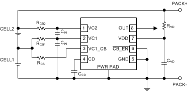
The bq2920x device is a secondary overvoltage protection IC for 2-series cell lithium-ion battery packs that incorporates a high-accuracy precision overvoltage detection circuit and automatic cell imbalance correction.
The voltage of each cell in a 2-series cell battery pack is compared to a factory programmed internal reference voltage. If either cell reaches an overvoltage condition, the OUT pin changes from low to high state.
The bq2920x can perform automatic voltage-based cell imbalance correction. Balancing can start when the cell voltages are different by nominally 30 mV or more and stops when the difference is nominally 0 mV. Cell balancing is enabled and disabled by the CB_EN pin.
Device Information(1)
| PART NUMBER | PACKAGE | BODY SIZE (NOM) |
|---|---|---|
| bq29200 | VSON (8) | 3.00 mm × 3.00 mm |
| bq29209 |
- For all available packages, see the orderable addendum at the end of the datasheet.
