SLUSA52C September   2010  – March 2016

PRODUCTION DATA.  

  1. Features
  2. Applications
  3. Description
  4. Revision History
  5. Device Options
  6. Pin Configuration and Functions
  7. Specifications
    1. 7.1 Absolute Maximum Ratings
    2. 7.2 ESD Ratings
    3. 7.3 Recommended Operating Conditions
    4. 7.4 Thermal Information
    5. 7.5 Electrical Characteristics
    6. 7.6 Recommended Cell Balancing Configurations
    7. 7.7 Typical Characteristics
  8. Detailed Description
    1. 8.1 Overview
      1. 8.1.1 Voltage Protection
      2. 8.1.2 Cell Balancing
    2. 8.2 Functional Block Diagram
    3. 8.3 Feature Description
      1. 8.3.1 Protection (OUT) Timing
      2. 8.3.2 Cell Voltage > VPROTECT
      3. 8.3.3 Cell Connection Sequence
      4. 8.3.4 Cell Balance Enable Control
      5. 8.3.5 Cell Balance Configuration
      6. 8.3.6 Cell Imbalance Auto-Detection (Via Cell Voltage)
      7. 8.3.7 Customer Test Mode
      8. 8.3.8 Test Conditions
    4. 8.4 Device Functional Modes
      1. 8.4.1 NORMAL Mode
      2. 8.4.2 PROTECTION Mode
  9. Application and Implementation
    1. 9.1 Application Information
    2. 9.2 Typical Applications
      1. 9.2.1 Battery Connection
        1. 9.2.1.1 Design Requirements
        2. 9.2.1.2 Detailed Design Procedure
        3. 9.2.1.3 Application Curve
    3. 9.3 System Example
      1. 9.3.1 External Cell Balancing
  10. 10Power Supply Recommendations
  11. 11Layout
    1. 11.1 Layout Guidelines
    2. 11.2 Layout Example
  12. 12Device and Documentation Support
    1. 12.1 Related Links
    2. 12.2 Community Resources
    3. 12.3 Trademarks
    4. 12.4 Electrostatic Discharge Caution
    5. 12.5 Glossary
  13. 13Mechanical, Packaging, and Orderable Information

Package Options

Refer to the PDF data sheet for device specific package drawings

Mechanical Data (Package|Pins)
  • DRB|8
Thermal pad, mechanical data (Package|Pins)
Orderable Information

6 Pin Configuration and Functions

DRB Package
8-Pin VSON
Top View
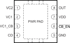
bq29200 bq29209 po_lusa52.gif

Pin Functions

PIN DESCRIPTION
NAME NO.
CB_EN 6 Cell balance enable
CD 4 Connection to external capacitor for programmable delay time
GND 5 Ground pin
OUT 8 Output
Thermal Pad PWR PAD GND pin to be connected to the PWRPAD on the printed circuit board for proper operation
VC1 2 Sense voltage input for bottom cell
VC1_CB 3 Cell balance input for bottom cell
VC2 1 Sense voltage input for top cell
VDD 7 Power supply