SLUSBS8B December 2013 – November 2019 BQ40Z50
PRODUCTION DATA.
- 1 Features
- 2 Applications
- 3 Description
- 4 Revision History
- 5 Description (continued)
- 6 Pin Configuration and Functions
-
7 Specifications
- 7.1 Absolute Maximum Ratings
- 7.2 ESD Ratings
- 7.3 Recommended Operating Conditions
- 7.4 Thermal Information
- 7.5 Electrical Characteristics: Supply Current
- 7.6 Electrical Characteristics: Power Supply Control
- 7.7 Electrical Characteristics: AFE Power-On Reset
- 7.8 Electrical Characteristics: AFE Watchdog Reset and Wake Timer
- 7.9 Electrical Characteristics: Current Wake Comparator
- 7.10 Electrical Characteristics: VC1, VC2, VC3, VC4, BAT, PACK
- 7.11 Electrical Characteristics: SMBD, SMBC
- 7.12 Electrical Characteristics: PRES, BTP_INT, DISP
- 7.13 Electrical Characteristics: LEDCNTLA, LEDCNTLB, LEDCNTLC
- 7.14 Electrical Characteristics: Coulomb Counter
- 7.15 Electrical Characteristics: CC Digital Filter
- 7.16 Electrical Characteristics: ADC
- 7.17 Electrical Characteristics: ADC Digital Filter
- 7.18 Electrical Characteristics: CHG, DSG FET Drive
- 7.19 Electrical Characteristics: PCHG FET Drive
- 7.20 Electrical Characteristics: FUSE Drive
- 7.21 Electrical Characteristics: Internal Temperature Sensor
- 7.22 Electrical Characteristics: TS1, TS2, TS3, TS4
- 7.23 Electrical Characteristics: PTC, PTCEN
- 7.24 Electrical Characteristics: Internal 1.8-V LDO
- 7.25 Electrical Characteristics: High-Frequency Oscillator
- 7.26 Electrical Characteristics: Low-Frequency Oscillator
- 7.27 Electrical Characteristics: Voltage Reference 1
- 7.28 Electrical Characteristics: Voltage Reference 2
- 7.29 Electrical Characteristics: Instruction Flash
- 7.30 Electrical Characteristics: Data Flash
- 7.31 Electrical Characteristics: OCD, SCC, SCD1, SCD2 Current Protection Thresholds
- 7.32 Timing Requirements: OCD, SCC, SCD1, SCD2 Current Protection Timing
- 7.33 Timing Requirements: SMBus
- 7.34 Timing Requirements: SMBus XL
- 7.35 Typical Characteristics
-
8 Detailed Description
- 8.1 Overview
- 8.2 Functional Block Diagram
- 8.3
Feature Description
- 8.3.1 Primary (1st Level) Safety Features
- 8.3.2 Secondary (2nd Level) Safety Features
- 8.3.3 Charge Control Features
- 8.3.4 Gas Gauging
- 8.3.5 Configuration
- 8.3.6 Battery Parameter Measurements
- 8.3.7 Battery Trip Point (BTP)
- 8.3.8 Lifetime Data Logging Features
- 8.3.9 Authentication
- 8.3.10 LED Display
- 8.3.11 Voltage
- 8.3.12 Current
- 8.3.13 Temperature
- 8.3.14 Communications
- 8.4 Device Functional Modes
- 9 Applications and Implementation
- 10Power Supply Recommendations
- 11Layout
- 12Device and Documentation Support
- 13Mechanical, Packaging, and Orderable Information
Package Options
Mechanical Data (Package|Pins)
- RSM|32
Thermal pad, mechanical data (Package|Pins)
- RSM|32
Orderable Information
9.2.2.2.3 System Present
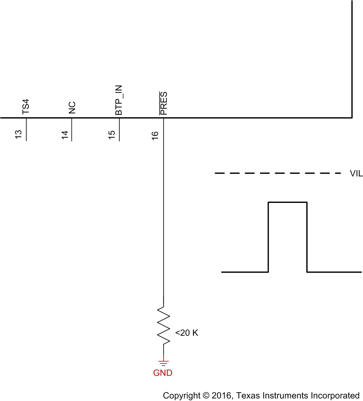
The System Present signal is used to inform the gas gauge whether the pack is installed into or removed from the system. In the host system, this pin is grounded. The PRES pin of the BQ40Z50 is occasionally sampled to test for system present. To save power, an internal pullup is provided by the gas gauge during a brief 4-μs sampling pulse once per second. A resistor can be used to pull the signal low and the resistance must be 20 kΩ or lower to insure that the test pulse is lower than the VIL limit. The pull-up current source is typically 10 µA to 20 µA.
 Figure 28. System Present Pull-Down Resistor
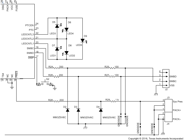
 Because the System Present signal is part of the pack connector interface to the outside world, it must be protected from external electrostatic discharge events. An integrated ESD protection on the PRES device pin reduces the external protection requirement to just R29 for an 8-kV ESD contact rating. However, if it is possible that the System Present signal may short to PACK+, then R28 and D4 must be included for high-voltage protection.
 Figure 29. System Present ESD and Short Protection