SLUSAW3D December 2014 – January 2017
PRODUCTION DATA.
- 1 Features
- 2 Applications
- 3 Description
- 4 Revision History
- 5 Description (continued)
- 6 Pin Configuration and Functions
-
7 Specifications
- 7.1 Absolute Maximum Ratings
- 7.2 ESD Ratings
- 7.3 Recommended Operating Conditions
- 7.4 Thermal Information
- 7.5 Supply Voltage
- 7.6 Supply Current
- 7.7 Power Supply Control
- 7.8 Low-Voltage General Purpose I/O (TSx)
- 7.9 High-Voltage General Purpose I/O (GPIO0, GPIO1)
- 7.10 AFE Power-On Reset
- 7.11 Internal 1.8-V LDO
- 7.12 Current Wake Comparator
- 7.13 Coulomb Counter
- 7.14 CC Digital Filter
- 7.15 ADC
- 7.16 ADC Digital Filter
- 7.17 ADC Multiplexer
- 7.18 Cell Balancing Support
- 7.19 Cell Detach Detection
- 7.20 Internal Temperature Sensor
- 7.21 NTC Thermistor Measurement Support (ADCx)
- 7.22 High-Frequency Oscillator
- 7.23 Low-Frequency Oscillator
- 7.24 Voltage Reference 1
- 7.25 Voltage Reference 2
- 7.26 Instruction Flash
- 7.27 Data Flash
- 7.28 Current Protection Thresholds
- 7.29 N-CH FET Drive (CHG, DSG)
- 7.30 FUSE Drive (AFEFUSE)
- 7.31 Battery Charger Voltage Regulation (VFB)
- 7.32 Battery Charger Current Sense (HSRP, HSRN)
- 7.33 Battery Charger Precharge Current Sense (HSRP, HSRN)
- 7.34 AC Adapter Fault Detect (HSRN, VCC)
- 7.35 Battery Charger Overcurrent Detection (V)HSRP, (V)HSRN
- 7.36 Battery Charger Undercurrent Detection (V)HSRP, (V)HSRN
- 7.37 System Operation Detection (V)HSRN
- 7.38 Battery Overvoltage Comparator (VFB)
- 7.39 Regulator (REGN)
- 7.40 PWM High-Side Driver (HiDRV)
- 7.41 PWM Low-Side Driver (LoDRV)
- 7.42 PWM Information
- 7.43 Charger Power-Up Sequence
- 7.44 Thermal Shutdown Comparator
- 7.45 SMBus High Voltage I/O
- 7.46 SMBus
- 7.47 SMBus XL
- 7.48 Timing Requirements
- 7.49 Typical Characteristics
-
8 Detailed Description
- 8.1 Overview
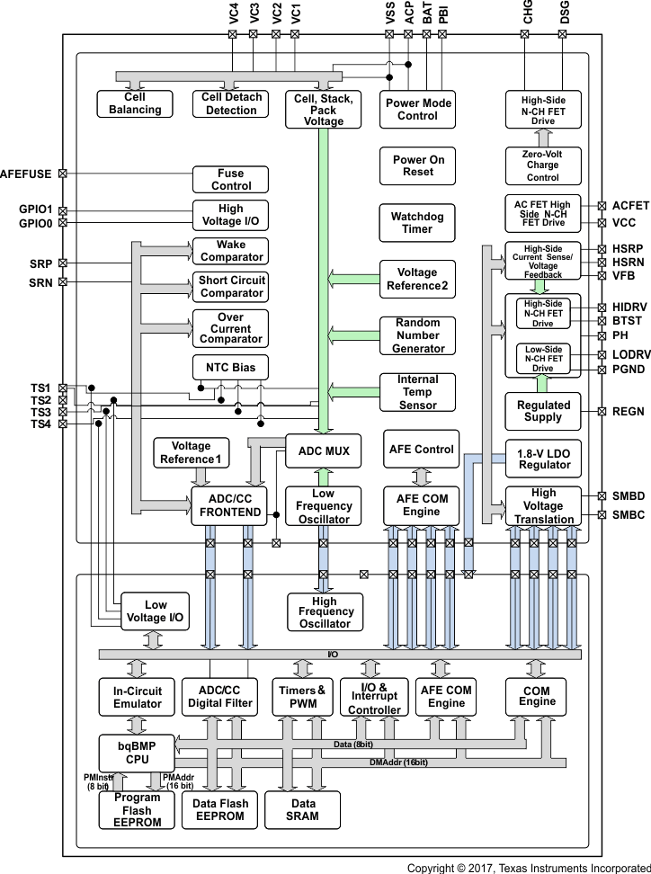
- 8.2 Functional Block Diagram
- 8.3 Feature Description
- 9 Application and Implementation
- 10Power Supply Recommendations
- 11Layout
- 12Device and Documentation Support
- 13Mechanical, Packaging, and Orderable Information
Package Options
Mechanical Data (Package|Pins)
- RHB|32
Thermal pad, mechanical data (Package|Pins)
- RHB|32
Orderable Information
8 Detailed Description
8.1 Overview
The bq40z60 is a fully integrated battery manager that employs flash-based firmware and integrated hardware protection to provide a complete solution for 2-series to 4-series cell battery stack architectures. The bq40z60 interfaces with a host system via an SBS v1.1-compliant SMBus interface, and processes instructions and data using a state-of-the-art, ultra-low-power TI bqBMP CPU. High-performance, integrated analog peripherals enable support for a sense resistor down to 5 mΩ, battery charge control, and simultaneous current/voltage data conversion for instant power calculations.
The bq40z60 controls the cell charging profile based on user-programmed data flash parameters for charging current and voltage based on temperature and cell voltage. The gas gauge provides the cell voltage and charging information to the battery charging through an internal communication bus. The charger function is controlled based on cell voltage measurements both on individual cell and total series stack readings.
The analog front end provides this voltage-based information to the charging circuit to set the profiles pre-programmed in the data flash settings, which are useful for zero voltage and PRECHARGE mode operation. The following sections detail all of the major component blocks in the bq40z60 device.
8.3 Feature Description
The bq40z60 consists of an integrated analog front end, charge controller, and fuel gauge. The following sections provide an overview of the device features. For additional details, refer to the bq40z60 Technical Reference Manual (SLUUA04).
8.3.1 Safety Features
The bq40z60 provides support for primary safety, including:
- Cell Over/Undervoltage Protection
- Charge and Discharge Overcurrent
- Short Circuit Protection
- Charge and Discharge Overtemperature
The secondary safety features of the bq40z60 can be used to indicate more serious faults via the FUSE pin. This pin can be used to blow an in-line fuse to permanently disable the battery pack from charging or discharging. The secondary safety features provide protection against:
- Safety Over/Undervoltage Permanent Failure
- Safety Overtemperature Permanent Failure
- Safety FET Overtemperature Permanent Failure
- Qmax Imbalance Permanent Failure
- Impedance Imbalance Permanent Failure
- Capacity Degradation Permanent Failure
- Cell Balancing Permanent Failure
- Fuse Failure Permanent Failure
- Voltage Imbalance at Rest Permanent Failure
- Voltage Imbalance Active Permanent Failure
- Charge/Discharge FET Permanent Failure
- Second Level Protector Permanent Failure
- Instruction Flash Checksum Permanent Failure
- Open Cell Connection Permanent Failure
- Data Flash Permanent Failure
- Open Thermistor Permanent Failure
8.3.2 Analog Front End (AFE) Details
The analog front end (AFE) consists of circuits responsible for managing internal power and interfacing to outside components for measuring current, voltage, and temperature. The bq40z60 AFE includes an active-high interrupt output connected internally to the fuel gauge to notify it of important changes in some of the AFE registers.
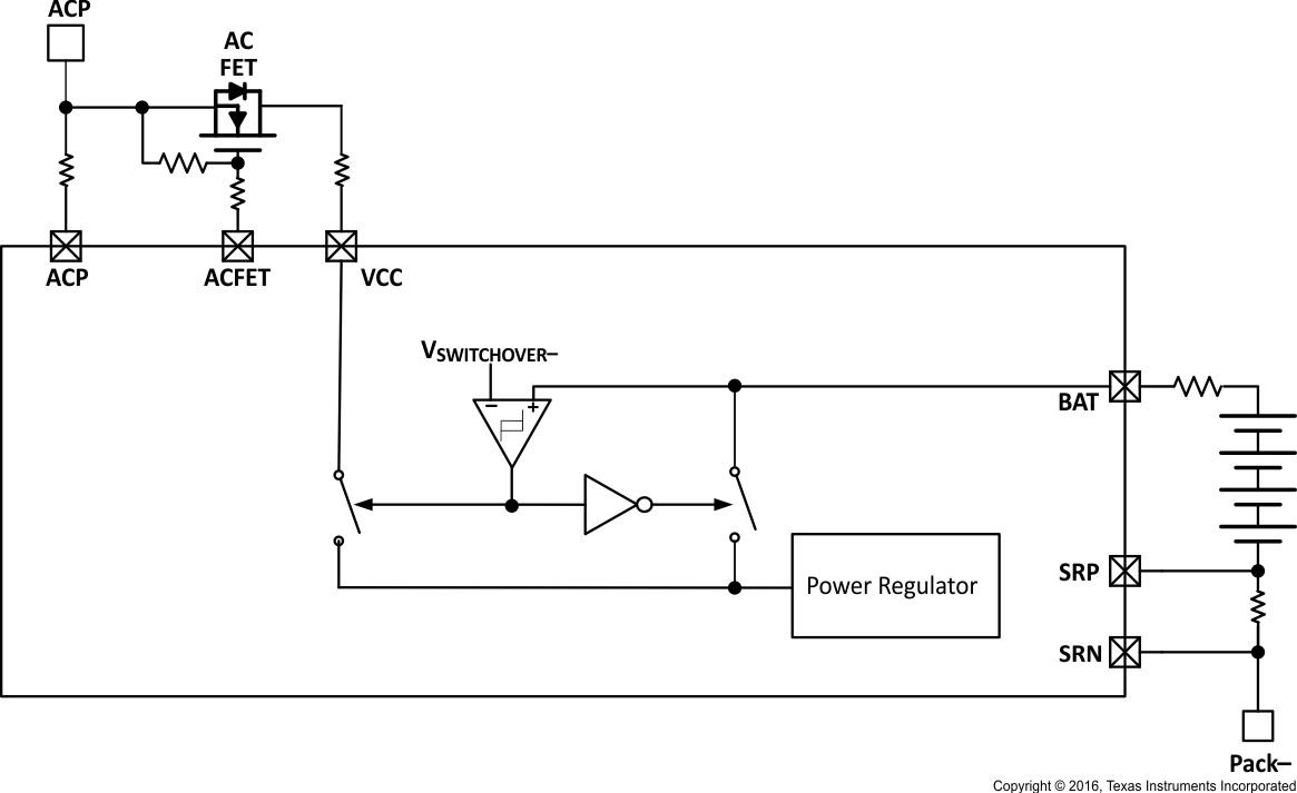
The bq40z60 manages its supply voltage dynamically according to operating conditions. When VBAT > VSWITCHOVER– + VHYS, the AFE connects an internal switch to BAT and uses this pin to supply power to its internal 1.8-V LDO, which subsequently powers all device logic and flash operations. Once BAT decreases to VBAT < VSWITCHOVER–, the AFE disconnects its internal switch from BAT and connects another switch to VCC, allowing sourcing of power from a charger (if present). An external capacitor connected to PBI provides a momentary supply voltage to help guard against system brownouts due to transient short-circuit or overload events that pull VBAT below VSWITCHOVER–.
In the event of a power-cycle, the bq40z60 AFE will hold its internal RESET output pin high for tRST duration to allow its internal 1.8-V LDO and LFO to stabilize before running the analog gas gauge (AGG). The AFE enters power-on reset when the voltage at VREG falls below VREGIT–, and exits reset when VREG rises above VREGIT– + VHYS for tRST time. After tRST, the bq40z60 AGG writes its trim values to the AFE.
 Figure 3. Power-On Reset Operation
The bq40z60 AFE includes a low frequency oscillator (LFO) running at 262.144 kHz. The AFE monitors the LFO frequency and indicates a failure via LATCH_STATUS[LFO] if the output frequency is much lower than normal.
The bq40z60 AFE provides two internal voltage references: VREF1, used by the ADC and CC, and VREF2 used by the LDO, LFO, current wake comparator, and over- and short-current protection circuitry.
8.3.2.1 Wake Up Comparator
The internal wake comparator can be used to wake the bq40z60 from a HALT state if a configurable threshold is detected across SRP and SRN.
8.3.2.2 Cell Balancing Support
The integrated cell balancing FETs included in the bq40z60 device allow the AFE to bypass cell current around a given cell or numerous cells to effectively balance the entire battery stack. External series resistors placed between the cell connections and the VCx input pins set the balancing current magnitude. The cell balancing circuitry can be enabled or disabled via the CELL_BAL_DET[CB3, CB2, CB1] control register. Series input resistors between 100 Ω and 1 kΩ are recommended for effective cell balancing.
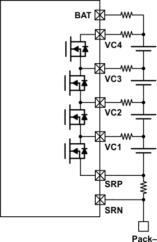 Figure 4. Cell Balancing Configuration
8.3.2.3 FET Drive
The bq40z60 controls two external N-CH MOSFETs in a back-to-back configuration for battery protection. The charge (CHG) and discharge (DSG) FETs are automatically disabled if a safety fault is detected and can also be manually turned off using AFE_CONTROL[CHGEN, DSGEN] = 0, 0. When the gate drive is disabled, an internal circuit discharges CHG to BAT and DSG to HSRN.
The AC FET (N-CH MOSFET) controls power input from the AC adaptor to the battery charging system by monitoring the voltage at the VCC pin, and turning ON the ACFET if the voltage exceeds the VHSRN voltage. The following register command sets the AC FET gate drive output control, AFE_STATUS register (0x01) ACFET (Pin 2): Setting this pin to 1 allows the AC FET gate drive to be on if other conditions are satisfied.
8.3.2.4 Fuse Drive
The bq40z60 AFE has the ability to blow an external fuse in the event of a permanent failure. The fuse drive itself is supplied from the BAT input pin and its state can be monitored using the AFE_STATUS[FUSE_RAW] register. If AFE_STATUS[FUSE_RAW} = 1 for tDELAY duration, then LATCH_STATUS[FUSE] is set to 1, and after an additional 500 ms, the CHG and DSG FET drive outputs will be disabled if LATCH_STATUS[FUSE] has not been cleared by then. If the AFEFUSE output is not used, it should be connected to VSS. When AFEFUSE is in the low state, it uses an internal weak pullup to enable detection of disconnection between the AFEFUSE pin and the fuse drive circuitry.
8.3.3 Charge Controller Details
The charge controller, under control from the fuel gauge's processor, provides autonomous control over the charging of the battery pack. The controller uses a 1-MHz buck architecture using external FETs driven by internal gate drivers. The charge voltage and current can be adjusted via data flash values to account for the temperature and voltage of the battery cells, allowing for a JEITA type charge profile. The voltage and current may also be directly written to the charge controller from an external host, allowing for a user-defined charging profile. The charger runs in Narrow Voltage DC, that is, the output voltage of the charger will only exceed the battery voltage by a small amount; by contrast, a charger that does not run in Narrow Voltage DC mode will output the adapter voltage to the system.
The charger is designed to enable the system to continue to run while the battery is charged. If the system requires more current than the charger is able to provide, the battery supplements the current to the system. The charger can support an external precharge FET, allowing the VSYS to remain above a minimum voltage needed for the system to operate.
The charger supports precharge, constant current/constant voltage, and termination, as shown below. The voltage and current thresholds for precharge and termination are controlled by data flash values. Refer to the bq40z60 Technical Reference Manual (SLUUA04) for more information.
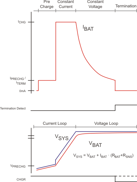 Figure 5. Normal Charge Profile
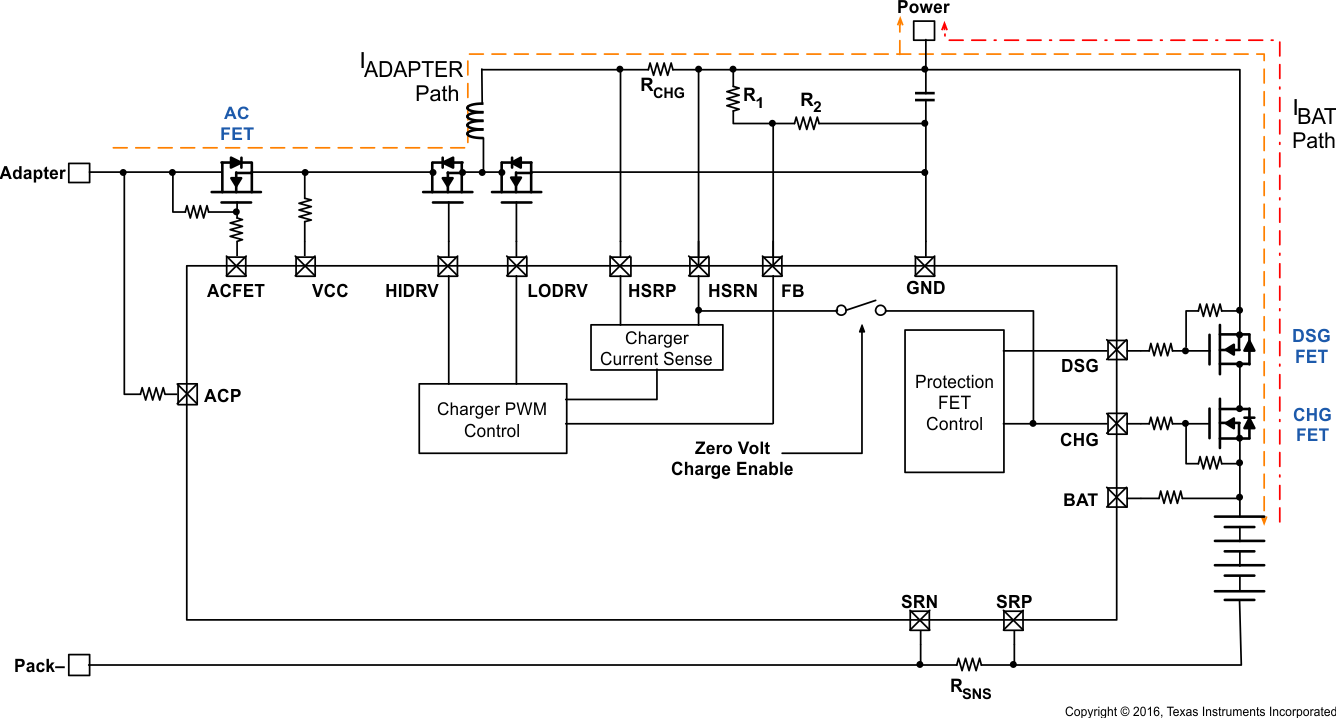
The charger maintains a cycle-by-cycle current limit by sensing across a resistor in series with the inductor (shown in Figure 6 as RCHG). In precharge and constant voltage, the DC current is regulated by sensing the current across the sense resistor at the bottom on of the cell stack. When the charger is enabled, the initial current is set for either the Precharge or Constant Current/Constant Voltage (CC/CV) value, based on the minimum cell voltage. Once the charger enters CONSTANT CURRENT mode, the temperature and maximum cell voltage-adjusted–charging current is set, and the voltage output of the charger is automatically regulated to maintain the current across RCHG. Once the temperature-adjusted voltage is reached by the charger output, the current starts to taper.
Throughout the charge cycle, the current available from the charger is limited by the ChargingCurrent() value. The system draws more current, however, with the battery supplementing the difference. Once battery charging is terminated, the charger is capable of supplying all of the current defined by the Advanced Charge Algorithm:Maximum Current Register value. Refer to the bq40z60 Technical Reference Manual (SLUUA04) for more information.
Figure 6 shows the system power path with the adaptor current and battery current overlaid. Further information is available in Application and Implementation.
8.3.3.1 Precharge Modes
The charge controller is designed to allow for both internal precharge control and external precharge control. The device can operate in precharge with external FETs and a current limiting resistor. Refer to the bq40z60 Technical Reference Manual (SLUUA04) for more information.
8.3.3.2 Zero-Volt Charge Support
This mode of operation is similar to PRECHARGE mode switched charging, but with the charge FET operation in the saturation region. The NVDC out is connected to the CHG gate drive output internally to allow for precharge current from the charger through the CHG FET. This current is limited based on the value of the external Rsense (10-mΩ resistor the lowest precharge current = 200 mA). This will increase the power dissipation of the charge FET and will require thermal heat management and protection to ensure correct operation.
8.3.3.3 Charge Termination
Once the highest cell voltage reaches the value specified in the data flash, the charger output voltage will no longer increase and the current will start to taper. Once the highest cell voltage is within the Charge Term Voltage window and the measured current is below Charge Term Taper Current for 40 s or more, the charger will terminate by disabling the CHG FET and setting the appropriate flags. Refer to the bq40z60 Technical Reference Manual (SLUUA04) for more information.
The system can still provide load current from the battery pack if the adaptor current cannot support the system load. The diode of the CHG FET starts to conduct as the system voltage decreases to a point where the pack voltage is greater than the system regulation voltage – Vdiode. If the average discharge current is high, the system can turn ON the CHG FET for improved efficiency and minimized line losses during the discharge phase.
8.3.4 Fuel Gauge and Control Details
The bq40z60 uses the Impedance Track™ algorithm to measure and calculate the available capacity in battery cells. The bq40z60 accumulates a measure of charge and discharge currents and compensates the charge current measurement for the temperature and state-of-charge of the battery. The bq40z60 estimates self-discharge of the battery and also adjusts the self-discharge estimation based on temperature. The device also has TURBO BOOST mode support, which enables the bq40z60 to provide the necessary data for the MCU to determine what level of peak power consumption can be applied without causing a system reset or a transient battery voltage level spike to trigger termination flags. See the bq40z60 Technical Reference Manual (SLUUA04) for further details.
8.3.4.1 Battery Trip Point (BTP)
Required for WIN8 OS, the Battery Trip Point (BTP) feature indicates when the RSOC of a battery pack has depleted to a certain value set in a DF register. This feature allows a host to program two capacity-based thresholds that govern triggering a BTP interrupt on the BTP_INT pin, and setting or clearing the OperationStatus[BTP_INT] on the basis of RemainingCapacity().
An internal weak pullup is applied when the BTP feature is active. Depending on the system design, an external pullup may be required to put on the BTP_INT pin. See High-Voltage General Purpose I/O (GPIO0, GPIO1) for details.
8.3.4.2 Lifetime Data Logging Features
The bq40z60 offers lifetime data logging for several critical battery parameters. The following parameters are updated every 10 hours if a difference is detected between values in RAM and data flash:
- Maximum and Minimum Cell Voltages
- Maximum Delta Cell Voltage
- Maximum Charge Current
- Maximum Discharge Current
- Maximum Average Discharge Current
- Maximum Average Discharge Power
- Maximum and Minimum Cell Temperature
- Maximum Delta Cell Temperature
- Maximum and Minimum Internal Sensor Temperature
- Maximum FET Temperature
- Number of Safety Events Occurrences and the Last Cycle of the Occurrence
- Number of Valid Charge Termination and the Last Cycle of the Valid Charge Termination
- Number of Qmax and Ra Updates and the Last Cycle of the Qmax and Ra Updates
- Number of Shutdown Events
- Cell Balancing Time for Each Cell
- Total FW Runtime and Time Spent in Each Temperature Range
(This data is updated every 2 hours if a difference is detected.)
(This data is updated every 2 hours if a difference is detected.)
8.3.5 Authentication
The bq40z60 supports authentication by the host using SHA-1. More information about the algorithm can be found in the bq40z60 Technical Reference Manual (SLUUA04).
8.3.6 LED Display
The bq40z60 can drive a 4-segment LED display for remaining capacity indication and/or a permanent fail (PF) error code indication.
8.3.7 Internal Temperature Sensor
An internal temperature sensor is available on the bq40z60 to reduce the cost, power, and size of the external components necessary to measure temperature. It is available for connection to the ADC using the multiplexer, and is ideal for determining pack temperature during storage and IC temperature during normal operation.
8.3.8 External Temperature Sensor Support
Each of the TSx input pins can be enabled with an 18-kΩ (Typ.) linearization pullup resistor to support using a 10 kΩ (25°C) NTC external thermistor, such as the Semitec 103AT–2. One or more thermistors can be connected between VSS and the individual RCx pin. The analog measurement is then taken via the ADC through its input multiplexer. If a different thermistor type is required, then changes to the external support components may be required.
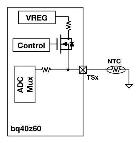 Figure 7. Thermistor Pin Configuration
8.3.9 High Frequency Oscillator
The bq40z60 includes a high frequency oscillator (HFO) running at 16.78 MHz. It is synthesized from the LFO output and scaled down to 8.388 MHz with 50% duty cycle. There is no need for external oscillator components.
8.3.10 Communications
The bq40z60 uses SMBus v1.1 with MASTER mode and packet error checking (PEC) options per the SBS specification.
8.3.10.1 SMBus On and Off State
The bq40z60 detects an SMBus off state when SMBC and SMBD are low for two or more seconds. Clearing this state requires that either SMBC or SMBD transition high. The communication bus will resume activity within 1 ms.
8.3.10.2 SBS Commands
The ManufacturerAccess() Command List shows the supported Manufacturer Access and SBS commands. See the bq40z60 Technical Reference Manual (SLUUA04) for further details.
Table 1. ManufacturerAccess() Command List
| FUNCTION | MANUFACTURER ACCESS COMMAND |
SBS COMMAND |
ACCESS | FORMAT | DATA READ ON 0x44 OR 0x23 | AVAILABLE IN SEALED MODE |
|---|---|---|---|---|---|---|
| DeviceType | 0x0001 | R | Block | Yes | Yes | |
| FirmwareVersion | 0x0002 | R | Block | Yes | Yes | |
| HardwareVersion | 0x0003 | R | Block | Yes | Yes | |
| IFChecksum | 0x0004 | R | Block | Yes | Yes | |
| StaticDFSignature | 0x0005 | R | Block | Yes | Yes | |
| ChemID | 0x0006 | R | Block | Yes | Yes | |
| StaticChemDFSignature | 0x0008 | R | Block | Yes | Yes | |
| AllDFSignature | 0x0009 | R | Block | Yes | Yes | |
| ShutdownMode | 0x0010 | W | — | — | Yes | |
| SleepMode | 0x0011 | W | — | — | — | |
| AutoCCOfset | 0x0013 | W | — | — | — | |
| FuseToggle | 0x001D | W | — | — | — | |
| PrechargeFET | 0x001E | W | — | — | — | |
| ChargeFET | 0x001F | W | — | — | — | |
| DischargeFET | 0x0020 | W | — | — | — | |
| Gauging | 0x0021 | W | — | — | — | |
| FETControl | 0x0022 | W | — | — | — | |
| LifetimeDataCollection | 0x0023 | W | — | — | — | |
| PermanentFailure | 0x0024 | W | — | — | — | |
| BlackBoxRecorder | 0x0025 | W | — | — | — | |
| Fuse | 0x0026 | W | — | — | — | |
| LifetimeDataReset | 0x0028 | W | — | — | — | |
| PermanentFailureData Reset |
0x0029 | W | — | — | — | |
| LifetimeDataFlush | 0x002E | W | — | — | — | |
| LifetimeDataSpeedUp Mode |
0x002F | W | — | — | — | |
| BlackBoxRecorderReset | 0x002A | W | — | — | — | |
| CalibrationMode | 0x002D | W | — | — | — | |
| SealDevice | 0x0030 | W | — | — | — | |
| SecurityKeys | 0x0035 | R/W | Block | Yes | — | |
| AuthenticationKey | 0x0037 | R/W | Block | — | — | |
| DeviceReset | 0x0041 | W | — | — | — | |
| SafetyAlert | 0x0050 | 0x50 | R | Block | Yes | Yes |
| SafetyStatus | 0x0051 | 0x51 | R | Block | Yes | Yes |
| PFAlert | 0x0052 | 0x52 | R | Block | Yes | Yes |
| PFStatus | 0x0053 | 0x53 | R | Block | Yes | Yes |
| OperationStatus | 0x0054 | 0x54 | R | Block | Yes | Yes |
| ChargingStatus | 0x0055 | 0x55 | R | Block | Yes | Yes |
| GaugingStatus | 0x0056 | 0x56 | R | Block | Yes | Yes |
| ManufacturingStatus | 0x0057 | 0x57 | R | Block | Yes | Yes |
| AFERegister | 0x0058 | 0x58 | R | Block | Yes | Yes |
| LifetimeDataBlock1 | 0x0060 | 0x60 | R | Block | Yes | Yes |
| LifetimeDataBlock2 | 0x0061 | 0x61 | R | Block | Yes | Yes |
| LifetimeDataBlock3 | 0x0062 | 0x62 | R | Block | Yes | Yes |
| ManufacturerInfo | 0x0070 | 0x70 | R | Block | Yes | Yes |
| DAStatus1 | 0x0071 | 0x71 | R | Block | Yes | Yes |
| DAStatus2 | 0x0072 | 0x72 | R | Block | Yes | Yes |
| GaugeStatus1 | 0x0073 | 0x73 | R | Block | Yes | Yes |
| GaugeStatus2 | 0x0074 | 0x74 | R | Block | Yes | Yes |
| GaugeStatus3 | 0x0075 | 0x75 | R | Block | Yes | Yes |
| StateofHealth | 0x0077 | R | Block | Yes | Yes | |
| CHGR_EN | 0x00C0 | W | — | — | No | |
| CVRD_ARM | 0x00C1 | W | — | — | Yes | |
| ACFETEST | 0x00C2 | W | — | — | No | |
| CHGONTEST | 0x00C3 | W | — | — | No | |
| ROMMode | 0x0F00 | W | — | — | — | |
| ExitCalibrationOutput | 0xF080 | R/W | Block | Yes | — | |
| OutputCCandADCfor Calibration |
0xF081 | R/W | Block | Yes | — | |
| OutputShortedCCand ADCforCalibration |
0xF082 | R/W | Block | Yes | — |
