SBOS765 January 2016
PRODUCTION DATA.
- 1 Features
- 2 Applications
- 3 Description
- 4 Revision History
- 5 Pin Configuration and Functions
- 6 Specifications
- 7 Detailed Description
- 8 Application and Implementation
- 9 Power Supply Recommendations
- 10Layout
- 11Device and Documentation Support
- 12Mechanical, Packaging, and Orderable Information
Package Options
Mechanical Data (Package|Pins)
- DCK|6
Thermal pad, mechanical data (Package|Pins)
Orderable Information
8 Application and Implementation
NOTE
Information in the following applications sections is not part of the TI component specification, and TI does not warrant its accuracy or completeness. TI’s customers are responsible for determining suitability of components for their purposes. Customers should validate and test their design implementation to confirm system functionality.
8.1 Application Information
The bq500100 is tailored to monitor current in wireless charging applications. This section focuses on the current-sense requirements for wireless charging. A typical application schematic and design procedure are provided in this section as reference.
8.2 Typical Application

NOTE:
RF1 = RF2 = RF8.2.1 Design Requirements
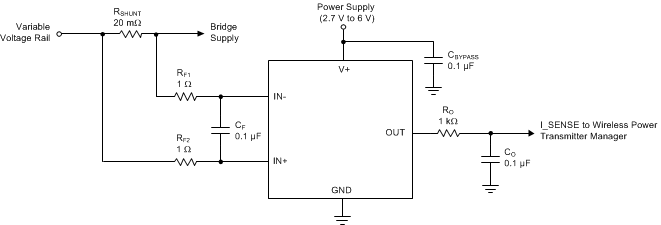
The design requirements for a typical wireless charging application is shown in Table 1. These requirements use the schematic shown in Figure 6.
Table 1. Design Parameters
| PARAMETER | DESIGN REQUIREMENT |
|---|---|
| Supply voltage range for V+ | 3.3 V ± 3% provided by a dc-dc converter |
| Common-mode voltage range | 9 V to 19 V provided by a dc-dc converter |
| Power loss in the shunt resistor | 20 mW or less at 1 A |
| Current-monitoring accuracy (gain error + offset error) | Better than 2.3% at 1 A, VCM = 12 V, TA = 25°C |
| I_SENSE peak-to-peak ripple | Less than 15 mV |
8.2.2 Detailed Design Procedure
The first step in designing a solution is to make sure that the supply voltage and common-mode voltage are within the specified operational range of the device. For the supply and common-mode voltage requirements specified in Table 1, the bq500100 reliably operates and is an ideal fit for this application.
The next step is to select the desired value for the shunt resistor. In this application example, the maximum power dissipation in the shunt resistor is specified to be 20 mW or less with a 1-A current-sense signal. The maximum power dissipation requirement limits the maximum value of the shunt resistor to 20 mW / (1 A)2, or 20 mΩ. To meet this application requirement and still maximize the current-sense accuracy, the maximum allowable resistance of 20 mΩ is selected.
Additional input filtering (see Figure 6) is required to mitigate the affects of differential noise and switching ripple because the device is sensing the voltage rail of the dc-dc supply. When adding series resistance to the input, keeping the resistance as small as possible is recommended because any added resistance adds to the gain error of the device. For the bq500100, the amount of additional gain error resulting from the filter resistance RS can be calculated using Equation 1:

Applying Equation 1 for the case where RF is equal to 1 Ω results in an additional gain error of 0.085%. Applying this result to the total gain error is calculated to be approximately 2.085%.
The total offset voltage can be calculated by adding the effects of drift, change in supply voltage, and change in the common-mode input voltage to the specified offset voltage. In this example, no additional errors need to be added to the common-mode voltage and temperature because the conditions specified in Table 1 match the VOS conditions specified in the Electrical Characteristics table. The only additional error that needs to be added to the offset voltage is the effect of changes to the supply voltage. This document specifies a supply voltage of 5 V; however, this application calls for a supply voltage of 3.3 V. The change in offset voltage resulting from the difference in supply voltage can be calculated by using the PSR specification in this document; see the Electrical Characteristics table. The PSRR of the device is typically ±0.1 μV/V; therefore, the change in offset voltage can be calculated by taking the difference in supply voltage and multiplying by this value. In this case, the supply voltage difference is 1.7 V (5 V – 3.3 V), so the change in offset voltage is 0.17 μV. Therefore the total offset voltage error is 150.17 µV. Because the offset voltage error is a fixed value, the percentage influence on the accuracy is a function of the load current and can be calculated by applying Equation 2.

Applying Equation 2 with an offset value of 150.15 µV, an RSHUNT value of 20 mΩ, and a shunt current of 1 A results in a percentage error of 0.751%.
Now that the total gain error and offset error of the device are known, the accuracy of the current-shunt monitor can be calculated with Equation 3:

Applying Equation 3 with a total gain error of 2.085% and a total offset error of 0.751% results in a total accuracy of 2.22% at 1 A, which is within the design target of 2.3%. Using a resistor tolerance of 0.5% to minimize errors introduced by RSHUNT is recommended.
Additional output filtering consisting of RO and CO (see Figure 6) is required to further reduce the ripple at the bq500100 current-sense output. For best performance, keeping the ripple on the current monitor output below 15 mV is recommended. The values provided in Figure 6 are sufficient for most use cases.
8.2.3 Application Curve
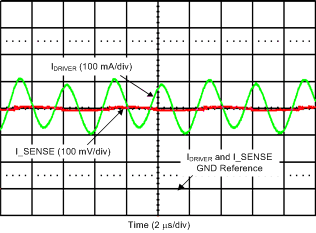
An example output response of the wireless charging application is shown in Figure 7.
The coil driver current is shown in green and has both ac and dc components. The I_SENSE signal is shown in red and is filtered to generate a signal representative of the dc current for foreign object detection.
 Figure 7. Current-Sense Output in a Wireless Charging Application