SLUSBD6D July 2013 – July 2016
PRODUCTION DATA.
- 1 Features
- 2 Applications
- 3 Description
- 4 Revision History
- 5 Pin Configuration and Functions
- 6 Specifications
-
7 Detailed Description
- 7.1 Overview
- 7.2 Functional Block Diagram
- 7.3 Feature Description
- 7.4 Device Functional Modes
- 7.5 Programming
- 8 Application and Implementation
- 9 Power Supply Recommendations
- 10Layout
- 11Device and Documentation Support
- 12Mechanical, Packaging, and Orderable Information
Package Options
Mechanical Data (Package|Pins)
- RGZ|48
Thermal pad, mechanical data (Package|Pins)
- RGZ|48
Orderable Information
7 Detailed Description
7.1 Overview
The principle of wireless power transfer is simply an open-cored transformer consisting of transmitter and receiver coils. The transmitter coil and electronics are typically built into a charger pad, and the receiver coil and electronics are typically built into a portable device such as a cell phone. When the receiver coil is positioned on the transmitter coil, magnetic coupling can occur when the transmitter coil is driven. The flux is coupled into the secondary coil, inducing a voltage, causing current to flow. The secondary voltage is rectified, allowing power to be transferred effectively to a load wirelessly. Power transfer can be managed through any of the various closed-loop control schemes.
7.2 Functional Block Diagram
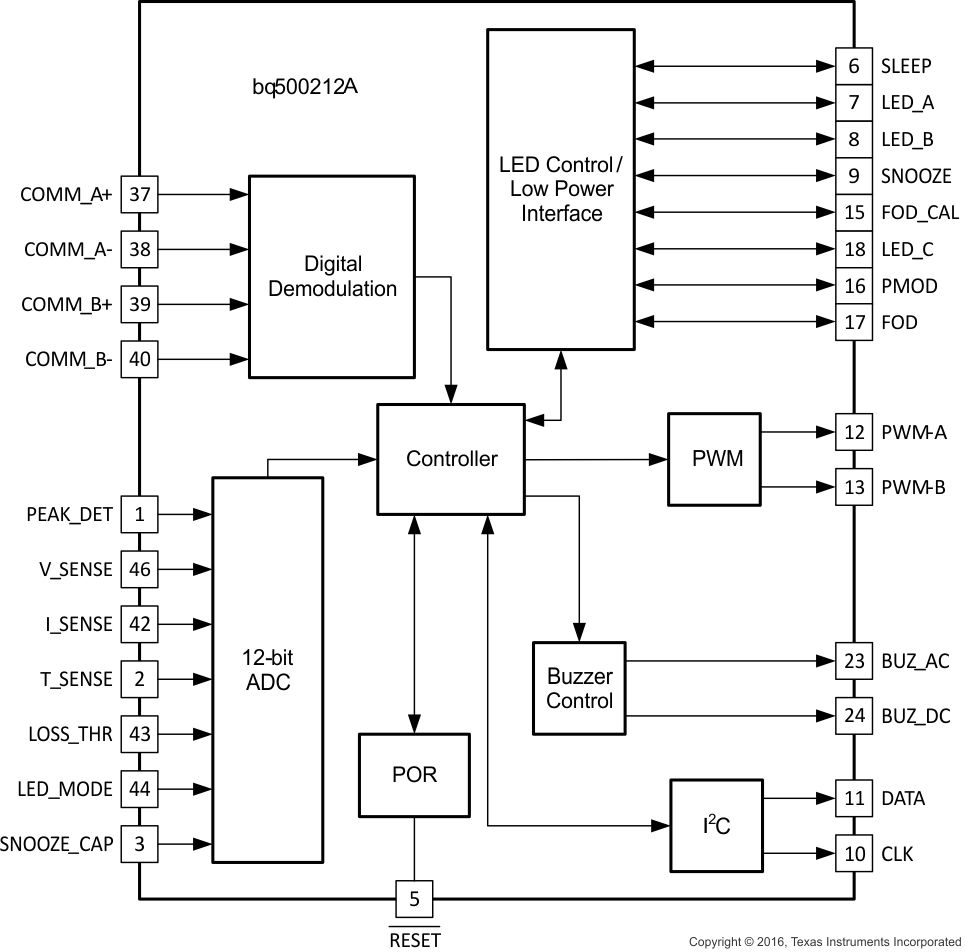
7.3 Feature Description
7.3.1 Principles of Operation
7.3.1.1 Fundamentals
The principle of wireless power transfer is simply an open-cored transformer consisting of primary and secondary coils and associated electronics. The primary coil and electronics are also referred to as the transmitter, and the secondary side the receiver. The transmitter coil and electronics are typically built into a charger pad. The receiver coil and electronics are typically built into a portable device, such as a cell phone.
When the receiver coil is positioned on the transmitter coil, magnetic coupling occurs when the transmitter coil is driven. The flux is coupled into the secondary coil which induces a voltage, current flows, it is rectified and power can be transferred quite effectively to a load wirelessly. Power transfer can be managed through any of various familiar closed-loop control schemes.
7.3.1.2 Wireless Power Consortium (WPC)
The Wireless Power Consortium (WPC) is an international group of companies from diverse industries. The WPC standard was developed to facilitate cross compatibility of compliant transmitters and receivers. The standard defines the physical parameters and the communication protocol to be used in wireless power. For more information, go to www.wirelesspowerconsortium.com.
7.3.1.3 Power Transfer
Power transfer depends on coil coupling. Coupling is dependant on the distance between coils, alignment, coil dimensions, coil materials, number of turns, magnetic shielding, impedance matching, frequency, and duty cycle.
Most importantly, the receiver and transmitter coils must be aligned for best coupling and efficient power transfer. The closer the space between the coils, the better the coupling, but the practical distance is set to be less than
5 mm (as defined within the WPC Specification) to account for housing and interface surfaces.
Shielding is added as a backing to both the transmitter and receiver coils to direct the magnetic field to the coupled zone. Magnetic fields outside the coupled zone do not transfer power. Thus, shielding also serves to contain the fields to avoid coupling to other adjacent system components.
Regulation can be achieved by controlling any one of the coil coupling parameters. For WPC compatibility, the transmitter coils and capacitance are specified and the resonant frequency point is fixed at 100 kHz. Power transfer is regulated by changing the operating frequency between 110 kHz to 205 kHz. The higher the frequency, the further from resonance and the lower the power. Duty cycle remains constant at 50% throughout the power band and is reduced only once 205 kHz is reached.
The WPC standard describes the dimension and materials of the coils. It also has information on tuning the coils to resonance. The value of the inductor and resonant capacitor are critical to proper operation and system efficiency.
7.3.1.4 Communication
Communication within the WPC is from the receiver to the transmitter, where the receiver tells the transmitter to send power and how much. In order to regulate, the receiver must communicate with the transmitter whether to increase or decrease frequency. The receiver monitors the rectifier output and using Amplitude Modulation (AM), sends packets of information to the transmitter. A packet is comprised of a preamble, a header, the actual message and a checksum, as defined by the WPC standard.
The receiver sends a packet by modulating an impedance network. This AM signal reflects back as a change in the voltage amplitude on the transmitter coil. The signal is demodulated and decoded by the transmitter side electronics and the frequency of its coil drive output is adjusted to close the regulation loop. The bq500212A device features internal digital demodulation circuitry.
The modulated impedance network on the receiver can either be resistive or capacitive. Figure 5 shows the resistive modulation approach, where a resistor is periodically added to the load and also shows the resulting change in resonant curve which causes the amplitude change in the transmitter voltage indicated by the two operating points at the same frequency. Figure 6 shows the capacitive modulation approach, where a capacitor is periodically added to the load and also shows the resulting amplitude change in the transmitter voltage.
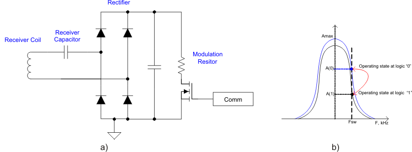 Figure 5. Receiver Resistive Modulation Circuit
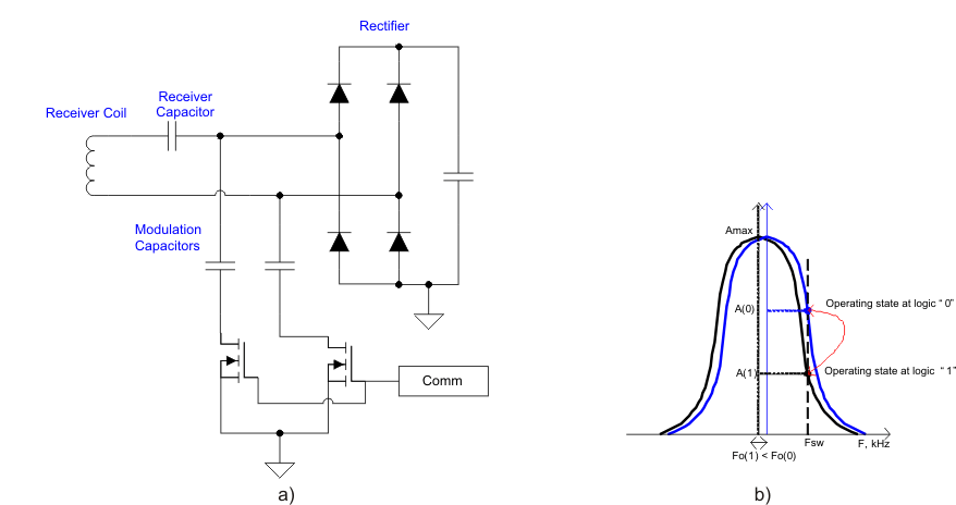 Figure 6. Receiver Capacitive Modulation Circuit
7.3.2 Dynamic Power Limiting
Dynamic Power Limiting (DPL) allows operation from a 5-V supply with limited current capability (such as a USB port). When the input voltage is observed drooping, the output power is dynamically limited to reduce the load and provides margin relative to the supply's capability.
Anytime the DPL control loop is regulating the operating point of the transmitter, the LED indicates that DPL is active. The LED color and flashing pattern are determined by the Table 2. If the receiver sends a Control Error Packet (CEP) with a negative value, (for example, to reduce power to the load), the WPTX in DPL mode responds to this CEP through the normal WPC control loop.
NOTE
The power limit indication depends on the LED_MODE selected.
7.3.3 Shut Down Through External Thermal Sensor or Trigger
Typical applications of the bq500212A device do not require additional thermal protection. This shutdown feature is provided for enhanced applications and is not only limited to thermal shutdown. The key parameter is the 1-V threshold on T_SENSE pin. Voltage below 1 V on T_SENSE pin for longer than 150 ms causes the device to shutdown.
The application of thermal monitoring through a Negative Temperature Coefficient (NTC) sensor, for example, is straightforward. The NTC forms the lower leg of a temperature dependant voltage divider. The NTC leads are connected to the bq500212A device, T_SENSE pin and GND. The threshold on T_SENSE pin is set to 1 V, below which the system shuts down and a fault is indicated (depending on LED mode chosen).
To implement this feature follow these steps:
- Consult the NTC data sheet and find the resistence vs temperature curve.
- Determine the actual temperature where the NTC is placed by using a thermal probe.
- Read the NTC resistance at that temperature in the NTC data sheet, that is R_NTC.
- Use Equation 1 to determine the upper leg resistor (R_Setpoint):

The system restores normal operation after approximately five minutes or if the receiver is removed. If the feature is not used, this pin must be pulled high.
NOTE
T_SENSE pin must always be terminated; otherwise, erratic behavior may result.
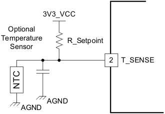 Figure 7. Negative Temperature Coefficient (NTC) Application
7.3.4 Fault Handling and Indication
Table 1 provides approximate durations for the time before a retry is attempted for end power transfer (EPT) packets and fault events. Precise timing may be affected by external components, or shortened by receiver removal. The LED mode selected determines how the LED indicates the condition or fault.
Table 1. Fault Handling
| CONDITION | DURATION (BEFORE RETRY) |
HANDLING |
|---|---|---|
| EPT-00 | Immediate | Unknown |
| EPT-01 | 5 s | Charge complete |
| EPT-02 | Infinite | Internal fault |
| EPT-03 | 5 minutes | Over temperature |
| EPT-04 | Immediate | Over voltage |
| EPT-05 | Immediate | Over current |
| EPT-06 | Infinite | Battery failure |
| EPT-07 | Not applicable | Reconfiguration |
| EPT-08 | Immediate | No response |
| OC (over current) | 1 minute | |
| NTC (external sensor) | 5 minutes | |
| PMOD/FOD warning | 12 s | 10 s LED only, 2 s LED + buzzer |
| PMOD/FOD | 5 minutes |
7.3.5 Power Transfer Start Signal
The bq500212A device features two signal outputs to indicate that power transfer has begun. BUZ_AC pin outputs a 400-ms duration, 4-kHz square wave for driving low-cost, AC-type ceramic buzzers. BUZ_DC pin outputs logic high, also for 400 ms, which is suitable for DC type buzzers with built-in tone generators, or as a trigger for any type of customized indication scheme. If not used, these pins can be left open.
7.3.6 Power On Reset
The bq500212A device has an integrated Power On Reset (POR) circuit which monitors the supply voltage and handles the correct device start-up sequence. Additional supply voltage supervisor or reset circuits are not needed.
7.3.7 External Reset, RESET Pin
The bq500212A device can be forced into a reset state by an external circuit connected to the RESET pin. A logic low voltage on this pin holds the device in reset. For normal operation, this pin is pulled up to 3.3 VCC with a 10-kΩ pullup resistor.
7.3.8 Trickle Charge and CS100
The WPC specification provides an End-of-Power Transfer message (EPT-01) to indicate charge complete. Upon receipt of the charge complete message, the bq500212A device changes the LED indication. The exact indication depends on the LED_MODE chosen.
In some battery charging applications there is a benefit to continue the charging process in trickle-charge mode to top off the battery. There are several information packets in the WPC specification related to the levels of battery charge (Charge Status). The bq500212A device uses these commands to enable top-off charging. The bq500212A device changes the LED indication to reflect charge complete when a Charge Status message is 100% received, but unlike the response to an EPT, it does not halt power transfer while the LED is solid green. The mobile device can use a CS100 packet to enable trickle charge mode.
If the reported charge status drops below 90% normal, charging indication is resumed.
7.4 Device Functional Modes
7.4.1 LED Indication Modes
The bq500212A device can directly drive up to three LED outputs (LED_A, LED_B, and LED_C) through a simple current limit resistor (typically 470 Ω), based on the mode selected. The current limit resistors can be individually adjusted to tune or match the brightness of the LEDs. Do not exceed the maximum output current rating of the device. The resistor in Figure 8 connected to LED_MODE and GND selects the desired LED indication scheme in Table 2.
- LED modes permit the use of one to three indicator LED's. Amber in the 2-LED mode is obtained by turning on both the green and red.
- LEDs can be turned on solid or configured to blink either slow (approximately 1.6 s period) or fast (approximately 400 ms period).
- Except in modes 2 and 9, the charge complete state is only maintained for 5 seconds after which it reverts to idle. This permits the processor to sleep in order to reduce standby power consumption. In other modes, external logic, such as a flip-flop, may be implemented to maintain the charge complete indication if desired.
Table 2. LED Modes
| LED CONTROL OPTION | LED SELECTION RESISTOR | DESCRIPTION | LED | OPERATIONAL STATES | |||||
|---|---|---|---|---|---|---|---|---|---|
| STANDBY | POWER TRANSFER | CHARGE COMPLETE | FAULT | DYNAMIC POWER LIMITING | FOD Warning | ||||
| X | < 36.5 kΩ | Reserved, do not use |
LED1, green | — | — | — | — | — | — |
| LED2, red | |||||||||
| LED3, amber | |||||||||
| 1 | 42.2 kΩ | Choice number 1 | LED1, green | Off | Blink slow | On | Off | Blink slow | Off |
| LED2, red | Off | Off | Off | On | Blink slow | Blink fast | |||
| LED3, amber | — | — | — | — | — | — | |||
| 2 | 48.7 kΩ | Choice number 2 | LED1, green | On | Blink slow | On | Off | Blink slow | Off |
| LED2, red | On | Off | Off | On | Blink slow | Blink fast | |||
| LED3, amber | — | — | — | — | — | — | |||
| 3 | 56.2 kΩ | Choice number 3 | LED1, green | Off | On | Off | Blink fast | On | On |
| LED2, red | — | — | — | — | — | — | |||
| LED3, amber | — | — | — | — | — | — | |||
| 4 | 64.9 kΩ | Choice number 4 | LED1, green | Off | On | Off | Off | Off | Off |
| LED2, red | Off | Off | Off | On | Blink slow | Blink fast | |||
| LED3, amber | — | — | — | — | — | — | |||
| 5 | 75 kΩ | Choice number 5 | LED1, green | Off | Off | On | Off | Off | Off |
| LED2, red | Off | On | Off | Off | On | On | |||
| LED3, amber | Off | Off | Off | Blink slow | Off | Off | |||
| 6 | 86.6 kΩ | Choice number 6 | LED1, green | Off | Blink slow | On | Off | Off | Off |
| LED2, red | Off | Off | Off | On | Off | Blink fast | |||
| LED3, amber | Off | Off | Off | Off | Blink Slow | Off | |||
| 7 | 100 kΩ | Choice number 7 | LED1, green | Off | Blink slow | Off | Off | Off | Off |
| LED2, red | Off | Off | On | Off | Off | Off | |||
| LED3, amber | Off | Off | Off | On | Blink slow | Blink fast | |||
| 8 | 115 kΩ | Choice number 8 | LED1, green | Off | Off | On | Blink slow | Off | Off |
| LED2, red | Off | On | Off | Blink slow | On | On | |||
| LED3, amber | — | — | — | — | — | — | |||
| 9 | 133 kΩ | Choice number 9 | LED1, green | Off | Blink slow | On | Off | Blink slow | Off |
| LED2, red | Off | Off | Off | On | Blink slow | Blink fast | |||
| LED3, amber | — | — | — | — | — | — | |||
| 10 | 154 kΩ | Choice number 10 | LED1, green | Off | On | Off | Blink fast | Blink slow | On |
| LED2, red | Off | Off | On | Off | Off | Off | |||
| LED3, amber | — | — | — | — | — | — | |||
7.4.2 Low Power Mode
During standby, when nothing is on the transmitter pad, the bq500212A device pings the surrounding environment at fixed intervals. The ping interval can be adjusted; the component values selected for the SNOOZE circuit determine this interval between pings. The choice of the ping interval effects two quantities: the idle efficiency of the system, and the time required to detect the presence of a receiver when it is placed on the pad. A trade-off must be made which balances low power (longest ping interval) with good user experience (quick detection through short ping interval) while still meeting the WPC requirement for detection within
0.5 seconds.
The system power consumption is approximately 300 mW during an active ping, which lasts approximately
90 ms, and 40 mW for the balance of the cycle. A weighted average can thus be used to estimate the overall system's idle consumption:
If T_ping is the interval between pings in ms, P_idle in mW is calculated with Equation 2.
7.5 Programming
7.5.1 Option Select Pins
Several pins on the bq500212A device are allocated to programming the FOD and PMOD Loss Threshold and the LED mode of the device. At power up, a bias current is applied to pins LED_MODE and LOSS_THR and the resulting voltage measured in order to identify the value of the attached programming resistor. The values of the operating parameters set by these pins are determined using Table 4. For LED_MODE, the selected bin determines the LED behavior based on Table 2; for the LOSS_THR, the selected bin sets a threshold used for PMOD (see PMOD, FOD, and FOD Calibration). See Table 2.
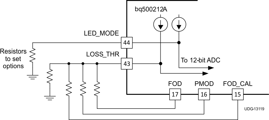 Figure 8. Option Select Pin Programming
7.5.2 Current Monitoring Requirements
The bq500212A device is WPC1.1 ready. To enable the FOD or PMOD features, current monitoring circuitry must be provided in the application design.
For proper scaling of the current monitor signal, the current sense resistor must be 20 mΩ and the current shunt amplifier must have a gain of 50, such as the INA199A1. For FOD accuracy, the current sense resistor must be a quality component with 1% tolerance, at least 1/4-W rating, and a temperature stability of ±200 PPM. Proper current sensing techniques in the application hardware must also be observed.
If WPC compliance is not required current monitoring can be omitted. Connect the I_SENSE pin to GND.
7.5.3 All Unused Pins
All unused pins can be left open unless otherwise indicated. The NC pin can be tied to GND and flooded with copper to improve ground shielding. See Pin Configuration and Functions for further more information.