SLUSBB8A December 2012 – June 2016
PRODUCTION DATA.
- 1 Features
- 2 Applications
- 3 Description
- 4 Revision History
- 5 Device Comparison Tables
- 6 Pin Configuration and Functions
- 7 Specifications
-
8 Detailed Description
- 8.1 Overview
- 8.2 Functional Block Diagram
- 8.3
Feature Description
- 8.3.1 Qi Wireless Power System and bq51010B Power Transfer Flow Diagrams
- 8.3.2 Dynamic Rectifier Control
- 8.3.3 Dynamic Efficiency Scaling
- 8.3.4 RILIM Calculations
- 8.3.5 Input Overvoltage
- 8.3.6 Adapter Enable Functionality and EN1 or EN2 Control
- 8.3.7 End Power Transfer Packet (WPC Header 0x02)
- 8.3.8 Status Outputs
- 8.3.9 WPC Communication Scheme
- 8.3.10 Communication Modulator
- 8.3.11 Adaptive Communication Limit
- 8.3.12 Synchronous Rectification
- 8.3.13 Temperature Sense Resistor Network (TS)
- 8.3.14 3-State Driver Recommendations For the TS-CTRL Pin
- 8.3.15 Thermal Protection
- 8.3.16 WPC 1.1 Compliance - Foreign Object Detection
- 8.4 Device Functional Modes
-
9 Application and Implementation
- 9.1 Application Information
- 9.2 Typical Applications
- 10Power Supply Recommendations
- 11Layout
- 12Device and Documentation Support
- 13Mechanical, Packaging, and Orderable Information
Package Options
Mechanical Data (Package|Pins)
- YFP|28
Thermal pad, mechanical data (Package|Pins)
Orderable Information
8 Detailed Description
8.1 Overview
The principle of the bq51010B wireless power transfer devices are simply to provide an open-cored transformer consisting of transmitter and receiver coils. The transmitter coil and electronics are built into a charger pad, and the receiver coil and electronics are typically built into a portable device such as a cell phone. When the receiver coil is positioned on the transmitter coil, magnetic coupling occurs when the transmitter coil is driven. The flux is coupled into the secondary coil, which induces a voltage and current flows. The secondary voltage is rectified, and power can be transferred effectively to a load wirelessly. Power transfer can be managed through any of the various closed-loop control schemes.
8.1.1 A Brief Description of the Wireless System
A wireless system consists of a charging pad (transmitter or primary) and the secondary-side equipment (receiver or secondary). There is a coil in the charging pad and in the secondary equipment which are magnetically coupled to each other when the secondary is placed on the primary. Power is then transferred from the transmitter to the receiver through coupled inductors (for example, an air-core transformer). Controlling the amount of power transferred is achieved by sending feedback (error signal) communication to the primary (for example, to increase or decrease power).
The receiver communicates with the transmitter by changing the load seen by the transmitter. This load variation results in a change in the transmitter coil current, which is measured and interpreted by a processor in the charging pad. Communication is done through digital-packets which are transferred from the receiver to the transmitter. Differential biphase encoding is used for the packets. The bit rate is 2-kbps.
Various types of communication packets have been defined. These include identification and authentication packets, error packets, control packets, end power packets, and power usage packets.
The transmitter coil stays powered off most of the time. It occasionally wakes up to see if a receiver is present. When a receiver authenticates itself to the transmitter, the transmitter remains powered on. The receiver maintains full control over the power transfer using communication packets.
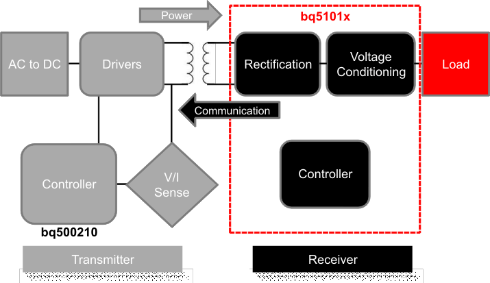 Figure 12. WPC Wireless Power System Indicating the Functional Integration of the bq51010B
8.2 Functional Block Diagram
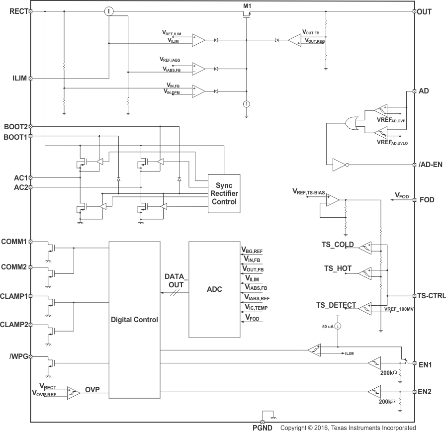
8.3 Feature Description
8.3.1 Qi Wireless Power System and bq51010B Power Transfer Flow Diagrams
The bq51010B family integrates a fully compliant WPC v1.1 communication algorithm to streamline receiver designs (no extra software development required). Other unique algorithms such has Dynamic Rectifier Control are also integrated to provide best-in-class system performance. This section provides a high-level overview of these features by illustrating the wireless power transfer flow diagram from start-up to active operation.
During start-up operation, the wireless power receiver must comply with proper handshaking to be granted a power contract from the TX. The TX initiates the hand shake by providing an extended digital ping. If an RX is present on the TX surface, the RX then provides the signal strength, configuration, and identification packets to the TX (see volume 1 of the WPC specification for details on each packet). These are the first three packets sent to the TX. The only exception is if there is a true shutdown condition on the EN1 or EN2, the AD, or the TS-CTRL pins where the RX shuts down the TX immediately (see Table 5 for details). Once the TX has successfully received the signal strength, configuration, and identification packets, the RX is granted a power contract and is then allowed to control the operating point of the power transfer. With the use of the Dynamic Rectifier Control algorithm, the RX informs the TX to adjust the rectifier voltage above 9 V prior to enabling the output supply. This method enhances the transient performance during system start-up (see Figure 13 for the start-up flow diagram details).
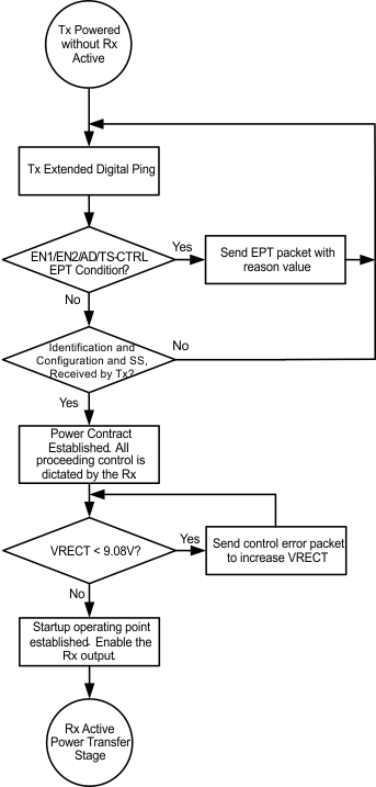 Figure 13. Wireless Power Start-Up Flow Diagram
Once the start-up procedure has been established, the RX enters the active power transfer stage. This is considered the main loop of operation. The Dynamic Rectifier Control algorithm determines the rectifier voltage target based on a percentage of the maximum output current level setting (set by KIMAX and the ILIM resistance to GND). The RX sends control error packets to converge on these targets. As the output current changes, the rectifier voltage target dynamically changes. As a note, the feedback loop of the WPC system is relatively slow where it can take up to 90 ms to converge on a new rectifier voltage target. It must be understood that the instantaneous transient response of the system is open loop and dependent on the RX coil output impedance at that operating point. The main loop also determines if any conditions in Table 5 are true to discontinue power transfer. See Figure 14 which illustrates the active power transfer loop.
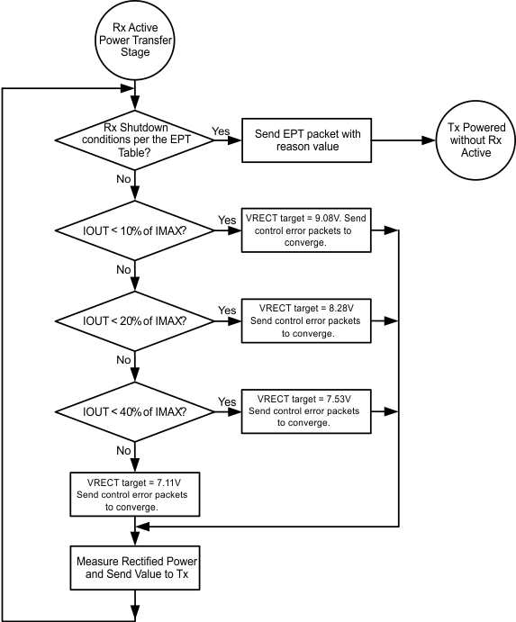 Figure 14. Active Power Transfer Flow Diagram
Another requirement of the WPC v1.1 specification is to send the measured recieved power. This task is enabled on the IC by measuring the voltage on the FOD pin which is proportional to the output current and can be scaled based on the choice of the resitor to ground on the FOD pin.
8.3.2 Dynamic Rectifier Control
The dynamic rectifier control algorithm offers the end system designer optimal transient response for a given max output current setting. This is achieved by providing enough voltage headroom across the internal regulator at light loads to maintain regulation during a load transient. The WPC system has a relatively slow global feedback loop where it can take more than 90 ms to converge on a new rectifier voltage target. Therefore, the transient response is dependent on the loosely coupled transformers output impedance profile. The dynamic rectifier control allows for a 2-V change in rectified voltage before the transient response is observed at the output of the internal regulator (output of the bq51010B). A 720-mA application allows up to a 1.5-Ω output impedance.
8.3.3 Dynamic Efficiency Scaling
The dynamic efficiency scaling feature allows for the loss characteristics of the bq51010B to be scaled based on the maximum expected output power in the end application. This effectively optimizes the efficiency for each application. This feature is achieved by scaling the loss of the internal LDO based on a percentage of the maximum output current. Note that the maximum output current is set by the KIMAX term and the RILIM resistance (where RILIM = KIMAX / IMAX). The flow diagram show in Figure 14 illustrates how the rectifier is dynamically controlled (Dynamic Rectifier Control) based on a fixed percentage of the IMAX setting. Table 2 summarizes how the rectifier behavior is dynamically adjusted based on two different RILIM settings.
Table 2. Dynamic Efficiency Scaling
| OUTPUT CURRENT PERCENTAGE | RILIM = 890 Ω IMAX = 0.35 A |
RILIM = 417 Ω IMAX = 0.75 A |
VRECT |
|---|---|---|---|
| 0% to 10% | 0 A to 0.035 A | 0 A to 0.075 A | 9.08 V |
| 10% to 20% | 0.035 A to 0.07 A | 0.075 A to 0.150 A | 8.28 V |
| 20% to 40% | 0.07 A to 0.14 A | 0.150 A to 0.225 A | 7.53 V |
| >40% | >0.14 A | >0.225 A | 7.11 V |
8.3.4 RILIM Calculations
The bq51010B includes a means of providing hardware overcurrent protection by means of an analog current regulation loop. The hardware current limit provides an extra level of safety by clamping the maximum allowable output current (for example, a current compliance). The RILIM resistor size also sets the thresholds for the dynamic rectifier levels and thus providing efficiency tuning per the maximum system current of each application. Calculate the total RILIM resistance with Equation 1.
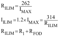
where
- IMAX is the expected maximum output current during normal operation
- IILIM is the hardware over current limit
When referring to the application diagram shown in Figure 27, RILIM is the sum of RFOD and the R1 resistance (for example, the total resistance from the ILIM pin to GND).
8.3.5 Input Overvoltage
If the input voltage suddenly increases in potential (for example, due to a change in position of the equipment on the charging pad), the voltage-control loop inside the bq51010B becomes active, and prevents the output from going beyond VOUT-REG. The receiver then starts sending back error packets to the transmitter every 30 ms until the input voltage comes back to the VRECT-REG target, and then maintains the error communication every 250 ms.
If the input voltage increases in potential beyond VOVP, the IC switches off the LDO and communicates to the primary to bring the voltage back to VRECT-REG. In addition, a proprietary voltage protection circuit is activated by means of CCLAMP1 and CCLAMP2 that protects the IC from voltages beyond the maximum rating of the IC (for example, 20 V).
8.3.6 Adapter Enable Functionality and EN1 or EN2 Control
Figure 32 is an example application that shows the bq51010B used as a wireless power receiver that can power multiplex between wired or wireless power for the down-system electronics. In the default operating mode pins EN1 and EN2 are low, which activates the adapter enable functionality. In this mode, if an adapter is not present the AD pin is low, and AD-EN pin is pulled to the higher of the OUT and AD pins so that the PMOS between OUT and AD is turned off. If an adapter is plugged in and the voltage at the AD pin goes above 3.6 V then wireless charging is disabled and the AD-EN pin is pulled approximately 4 V below the AD pin to connect AD to the secondary charger. The difference between AD and AD-EN is regulated to a maximum of 7V to ensure the VGS of the external PMOS is protected.
The EN1 and EN2 pins include internal 200-kΩ pulldown resistors, so that if these pins are not connected bq51010B defaults to AD-EN control mode. However, these pins can be pulled high to enable other operating modes as described in Table 3.
Table 3. EN/EN2 Control
| EN1 | EN2 | RESULT |
|---|---|---|
| 0 | 0 | Adapter control enabled. If adapter is present then secondary charger is powered by adapter, otherwise wireless charging is enabled when wireless power is available. Communication current limit is enabled. |
| 0 | 1 | Disables communication current limit. |
| 1 | 0 | AD-EN is pulled low, whether or not adapter voltage is present. This feature can be used, for example, in USB OTG applications. |
| 1 | 1 | Adapter and wireless charging are disabled, that is, power is never delivered by the OUT pin in this mode. |
Table 4. Adapter Enable Functionality
| EN1 | EN2 | WIRELESS POWER | WIRED POWER | OTG MODE | ADAPTIVE COMMUNICATION LIMIT | EPT |
|---|---|---|---|---|---|---|
| 0 | 0 | Enabled | Priority(1) | Disabled | Enabled | Not Sent to TX |
| 0 | 1 | Priority(1) | Enabled | Disabled | Disabled | Not Sent to TX |
| 1 | 0 | Disabled | Enabled | Enabled(2) | — | No Response |
| 1 | 1 | Disabled | Disabled | Disabled | — | Termination |
As described in Table 4, pulling EN2 high disables the adapter mode and only allows wireless charging. In this mode the adapter voltage is always blocked from the OUT pin. An application example where this mode is useful is when USB power is present at AD, but the USB is in suspend mode so that no power can be taken from the USB supply. Pulling EN1 high enables the off-chip PMOS regardless of the presence of a voltage. This function can be used in USB OTG mode to allow a charger connected to the OUT pin to power the AD pin. Finally, pulling both EN1 and EN2 high disables both wired and wireless charging.
NOTE
It is required to connect a back-to-back PMOS between AD and OUT so that voltage is blocked in both directions. Also, when AD mode is enabled no load can be pulled from the RECT pin as this could cause an internal device overvoltage in bq51010B.
8.3.7 End Power Transfer Packet (WPC Header 0x02)
The WPC allows for a special command for the receiver to terminate power transfer from the transmitter termed End Power Transfer (EPT) packet. Table 5 specifies the v1.1 reasons column and their corresponding data field value. The condition column corresponds to the methodology used by bq51010B to send equivalent message.
Table 5. End Power Transfer Packet
| MESSAGE | VALUE | CONDITION |
|---|---|---|
| Unknown | 0x00 | AD > 3.6 V |
| Charge Complete | 0x01 | TS/CTRL = 1, or EN1 = 1, or <EN1 EN2> = <11> |
| Internal Fault | 0x02 | TJ > 150°C or RILIM < 100 Ω |
| Over Temperature | 0x03 | TS < VHOT, TS > VCOLD, or TS/CTRL < 100 mV |
| Over Voltage | 0x04 | Not Sent |
| Over Current | 0x05 | NOT USED |
| Battery Failure | 0x06 | Not Sent |
| Reconfigure | 0x07 | Not Sent |
| No Response | 0x08 | VRECT target doesn't converge |
8.3.8 Status Outputs
The bq51010B has one status output, WPG. This output is an open-drain NMOS device that is rated to 20 V. The open-drain FET connected to the WPG pin is turned on whenever the output of the power supply is enabled. The output of the power supply is not enabled if the VRECT-REG does not converge at the no-load target voltage.
8.3.9 WPC Communication Scheme
The WPC communication uses a modulation technique termed back-scatter modulation where the receiver coil is dynamically loaded to provide amplitude modulation of the coil voltage and current of the transmitter. This scheme is possible due to the fundamental behavior between two loosely coupled inductors (for example, between the TX and RX coil). This type of modulation can be accomplished by switching in and out a resistor at the output of the rectifier, or by switching in and out a capacitor across the AC1/AC2 net. Figure 15 shows how to implement resistive modulation.
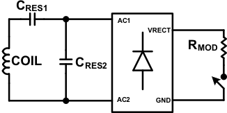 Figure 15. Resistive Modulation
Figure 16 shows how to implement capacitive modulation.
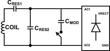 Figure 16. Capacitive Modulation
The amplitude change in TX coil voltage or current can be detected by the transmitters decoder. Figure 17 shows the resulting signal observed by the TX.
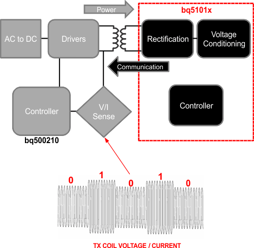 Figure 17. TX Coil Voltage and Current
The WPC protocol uses a differential biphase encoding scheme to modulate the data bits onto the TX coil voltage and current. Each data bit is aligned at a full period of 0.5 ms (tCLK) or 2 kHz. An encoded ONE results in two transitions during the bit period and an encoded ZERO results in a single transition. See Figure 18 for an example of the differential biphase encoding.
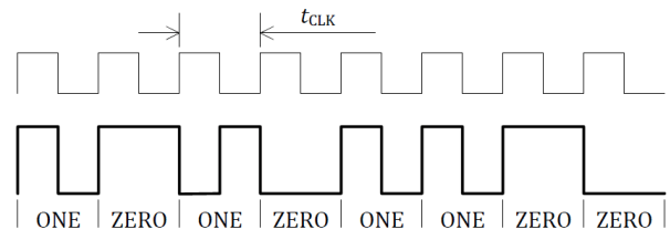 Figure 18. Differential Biphase Encoding Scheme (WPC volume 1: Low Power, Part 1 Interface Definition)
The bits are sent LSB first and use an 11-bit asynchronous serial format for each portion of the packet. This includes one start bit, n-data bytes, a parity bit, and a single stop bit. The start bit is always ZERO and the parity bit is odd. The stop bit is always ONE. Figure 19 shows the details of the asynchronous serial format.
 Figure 19. Asynchronous Serial Formatting (WPC volume 1: Low Power, Part 1 Interface Definition)
Each packet format is organized as shown in Figure 20.
 Figure 20. Packet Format (WPC volume 1: Low Power, Part 1 Interface Definition)
8.3.10 Communication Modulator
The bq51010B provides two identical, integrated communication FETs which are connected to the pins COM1 and COM2. These FETs are used for modulating the secondary load current which allows bq51010B to communicate error control and configuration information to the transmitter. Figure 21 below shows how the COMM pins can be used for resistive load modulation. Each COMM pin can handle at most a 24-Ω communication resistor. Therefore, if a COMM resistor between 12 Ω and 24 Ω is required COM1 and COM2 pins must be connected in parallel. bq51010B does not support a COMM resistor less than 12 Ω.
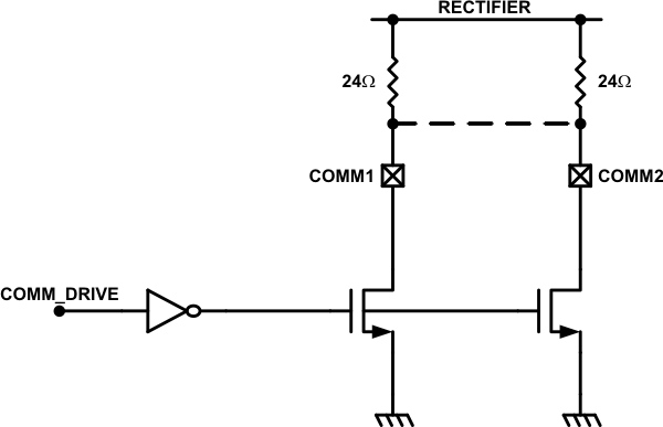 Figure 21. Resistive Load Modulation
In addition to resistive load modulation, the bq51010B is also capable of capacitive load modulation as shown in Figure 22 below. In this case, a capacitor is connected from COM1 to AC1 and from COM2 to AC2. When the COMM switches are closed there is effectively a 22-nF capacitor connected between AC1 and AC2. Connecting a capacitor in between AC1 and AC2 modulates the impedance seen by the coil, which is reflected in the primary as a change in current.
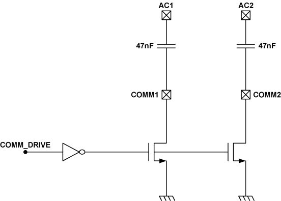 Figure 22. Capacitive Load Modulation
8.3.11 Adaptive Communication Limit
The Qi communication channel is established through backscatter modulation as described in the previous sections. This type of modulation takes advantage of the loosely coupled inductor relationship between the RX and TX coil. Essentially the switching in-and-out of the communication capacitor or resistor adds a transient load to the RX coil to modulate the TX coil voltage or current waveform (amplitude modulation). The consequence of this technique is that a load transient (load current noise) from the mobile device has the same signature. To provide noise immunity to the communication channel, the output load transients must be isolated from the RX coil. The proprietary feature adaptive communication limit achieves this by dynamically adjusting the current limit of the regulator. When the regulator is put in current limit, any load transients is offloaded to the battery in the system.
Note that this requires the battery charger IC to have input voltage regulation (weak adapter mode). The output of the RX appears as a weak supply if a transient occurs above the current limit of the regulator.
The adaptive communication limit feature has two current limit modes listed in Table 6.
Table 6. Adaptive Communication Limit
| IOUT | COMMUNICATION CURRENT LIMIT |
|---|---|
| < 300 mA | Fixed 400 mA |
| > 300 mA | IOUT + 50 mA |
8.3.12 Synchronous Rectification
The bq51010B provides an integrated, self-driven synchronous rectifier that enables high-efficiency AC to DC power conversion. The rectifier consists of an all NMOS H-Bridge driver where the backgates of the diodes are configured to be the rectifier when the synchronous rectifier is disabled. During the initial start-up of the WPC system the synchronous rectifier is not enabled. At this operating point, the DC rectifier voltage is provided by the diode rectifier. Once VRECT is greater than UVLO, half-synchronous mode is enabled until the load current surpasses 120 mA. Above 120 mA, the full synchronous rectifier stays enabled until the load current drops back below 100 mA where half-synchronous mode is enabled instead.
8.3.13 Temperature Sense Resistor Network (TS)
bq51010B includes a ratiometric external temperature sense function. The temperature sense function has two ratiometric thresholds which represent a hot and cold condition. TI recommends an external temperature sensor to provide safe operating conditions for the receiver product. This pin is best used for monitoring the surface that can be exposed to the end user (for example, place the NTC resistor closest to the user).
Figure 23 allows for any NTC resistor to be used with the given VHOT and VCOLD thresholds.
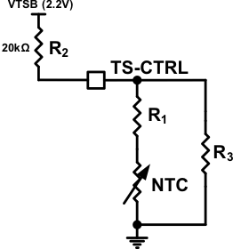 Figure 23. NTC Circuit Used for Safe Operation of the Wireless Receiver Power Supply
The resistors R1 and R3 can be solved by resolving the system of equations at the desired temperature thresholds (see Equation 2 and Equation 3).
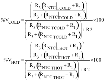

where
- TCOLD and THOT are the desired temperature thresholds in degrees Kelvin
- RO is the nominal resistance
- β is the temperature coefficient of the NTC resistor
- RO is fixed at 20 kΩ
An example solution is provided:
- R1 = 4.23 kΩ
- R3 = 66.8 kΩ
Where the chosen parameters are:
- %VHOT = 19.6%
- %VCOLD = 58.7%
- TCOLD = –10°C
- THOT = 100°C
- β = 3380
- RO = 10 kΩ
Figure 24 shows the plot of the percent VTSB vs temperature.
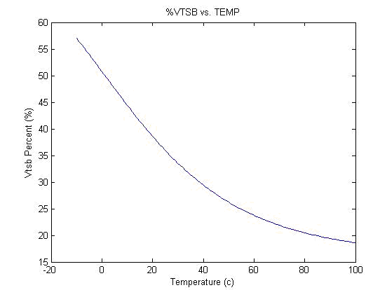 Figure 24. Example Solution for an NTC resistor with RO = 10 kΩ and β = 4500
Figure 25 illustrates the periodic biasing scheme used for measuring the TS state. The TS_READ signal enables the TS bias voltage for 24 ms. During this period the TS comparators are read (each comparator has a 10 ms deglitch) and appropriate action is taken based on the temperature measurement. After this 24 ms period has elapsed, the TS_READ signal goes low, which causes the TS-Bias pin to become high impedance. During the next 35 ms (priority packet period) or 235 ms (standard packet period), the TS voltage is monitored and compared to 100 mV. If the TS voltage is greater than 100 mV then a secondary device is driving the TS or CTRL pin and a CTRL = 1 is detected.
 Figure 25. Timing Diagram for TS Detection Circuit
8.3.14 3-State Driver Recommendations For the TS-CTRL Pin
The TS-CTRL pin offers three functions with one 3-state driver interface:
- NTC temperature monitoring,
- Fault indication,
- Charge done indication
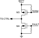 Figure 26. 3-state Driver for TS-CTRL
Note that the signals TERM and FAULT are given by two GPIOs. The truth table for this circuit is found in Table 7.
Table 7. Truth Table
| TERM | FAULT | F (RESULT) |
|---|---|---|
| 1 | 0 | Z (Normal mode) |
| 0 | 0 | Charge complete |
| 1 | 1 | System fault |
The default setting is TERM = 1 and FAULT = 0. In this condition, the TS-CTRL net is high impedance (hi-z); therefore, the NTC is function is allowed to operate. When the TS-CTRL pin is pulled to GND by setting
FAULT = 1, the RX is shutdown with the indication of a fault. When the TS-CTRL pin is pulled to the battery by setting TERM = 1, the RX is shutdown with the indication of a charge complete condition. Therefore, the host controller can indicate whether the RX is system is turning off due to a fault or due to a charge complete condition.
8.3.15 Thermal Protection
The bq51010B includes a thermal shutdown protection. If the die temperature reaches TJ(OFF), the LDO is shut off to prevent any further power dissipation. In this case bq51010B sends an EPT message of internal fault (0x02).
8.3.16 WPC 1.1 Compliance – Foreign Object Detection
The bq51010B is a WPC 1.1 compatible device. To enable a power transmitter to monitor the power loss across the interface as one of the possible methods to limit the temperature rise of foreign objects, the bq51010B reports its received power to the power transmitter. The received power equals the power that is available from the output of the power receiver plus any power that is lost in producing that output power (the power loss in the secondary coil and series resonant capacitor, the power loss in the shielding of the power receiver, the power loss in the rectifier). In WPC1.1 specification, foreign object detection (FOD) is enforced. This means the bq51010B sends received power information with known accuracy to the transmitter.
WPC 1.1 defines received power as “the average amount of power that the power receiver receives through its interface surface, in the time window indicated in the configuration packet".
To receive certification as a WPC 1.1 receiver, the Device Under Test (DUT) is tested on a reference transmitter whose transmitted power is calibrated, the receiver must send a received power such that Equation 4.
This 250-mW bias ensures that system remains interoperable.
WPC 1.1 transmitter is tested to see if they can detect reference foreign objects with a reference receiver.
WPC 1.1 specification allows much more accurate sensing of foreign objects.
8.4 Device Functional Modes
The operational modes of the bq51010B are described in Feature Description. The bq51010B has several functional modes. Start-up refers to the initial power transfer and communication between the receiver (bq51010B circuit) and the transmitter. Power transfer refers to any time that the TX and RX are communicating and power is being delivered from the TX to the RX. Power transfer termination occurs when the RX is removed from the TX, power is removed from the TX or the RX requests power transfer termination.