SLUSBX7C September 2014 – March 2017
PRODUCTION DATA.
- 1 Features
- 2 Applications
- 3 Description
- 4 Revision History
- 5 Device Comparison Table
- 6 Pin Configuration and Functions
- 7 Specifications
-
8 Detailed Description
- 8.1 Overview
- 8.2 Functional Block Diagram
- 8.3
Feature Description
- 8.3.1 Dynamic Rectifier Control
- 8.3.2 Dynamic Power Scaling
- 8.3.3 VO_REG Calculations
- 8.3.4 RILIM Calculations
- 8.3.5 Adapter Enable Functionality
- 8.3.6 Turning Off the Transmitter
- 8.3.7 Communication Current Limit
- 8.3.8 PD_DET and TMEM
- 8.3.9 TS/CTRL
- 8.3.10 PMODE Pin
- 8.3.11 I2C Communication
- 8.3.12 Input Overvoltage
- 8.3.13 Alignment Aid Using Frequency Information
- 8.4 Device Functional Modes
- 8.5
Register Maps
- 8.5.1 Wireless Power Supply Current Register 1
- 8.5.2 Wireless Power Supply Current Register 2
- 8.5.3 Wireless Power Supply Current Register 3
- 8.5.4 I2C Mailbox Register
- 8.5.5 I2C Mailbox Register 2
- 8.5.6 I2C Mailbox Register 3
- 8.5.7 Wireless Power Supply FOD RAM
- 8.5.8 Wireless Power User Header RAM
- 8.5.9 Wireless Power USER VRECT Status RAM
- 8.5.10 Wireless Power VOUT Status RAM
- 8.5.11 Wireless Power Proprietary Mode REC PWR MSByte Status RAM
- 8.5.12 Wireless Power REC PWR LSByte Status RAM
- 8.5.13 Wireless Power Prop Packet Payload RAM Byte 0
- 8.5.14 Wireless Power Prop Packet Payload RAM Byte 1
- 8.5.15 Wireless Power Prop Packet Payload RAM Byte 2
- 8.5.16 Wireless Power Prop Packet Payload RAM Byte 3
-
9 Application and Implementation
- 9.1 Application Information
- 9.2
Typical Applications
- 9.2.1
WPC v1.2 Power Supply 7-V Output With 1.4-A Maximum Current With I2C
- 9.2.1.1 Design Requirements
- 9.2.1.2
Detailed Design Procedure
- 9.2.1.2.1 Output Voltage Set Point
- 9.2.1.2.2 Output and Rectifier Capacitors
- 9.2.1.2.3 TMEM
- 9.2.1.2.4 Maximum Output Current Set Point
- 9.2.1.2.5 I2C
- 9.2.1.2.6 Communication Current Limit
- 9.2.1.2.7 Receiver Coil
- 9.2.1.2.8 Series and Parallel Resonant Capacitors
- 9.2.1.2.9 Communication, Boot, and Clamp Capacitors
- 9.2.1.3 Application Curves
- 9.2.2 Standalone 10-V WPC v1.2 Power Supply With 1-A Maximum Output Current in System Board
- 9.2.3
Standalone 10-V Power Supply With 1-A Maximum Output Current for 2S Charging System
- 9.2.3.1 Design Requirements
- 9.2.3.2
Detailed Design Procedure
- 9.2.3.2.1 Output Voltage Set Point
- 9.2.3.2.2 Output and Rectifier Capacitors
- 9.2.3.2.3 TMEM
- 9.2.3.2.4 Maximum Output Current Set Point
- 9.2.3.2.5 I2C
- 9.2.3.2.6 Communication Current Limit
- 9.2.3.2.7 Receiver Coil
- 9.2.3.2.8 Series Resonant Capacitors
- 9.2.3.2.9 Communication, Boot, and Clamp Capacitors
- 9.2.3.2.10 VRECT Clamp
- 9.2.3.3 Application Curves
- 9.2.1
WPC v1.2 Power Supply 7-V Output With 1.4-A Maximum Current With I2C
- 10Power Supply Recommendations
- 11Layout
- 12Device and Documentation Support
- 13Mechanical, Packaging, and Orderable Information
Package Options
Mechanical Data (Package|Pins)
- YFP|42
Thermal pad, mechanical data (Package|Pins)
Orderable Information
1 Features
- Robust 10-W Receiver Solution Using Proprietary Protocol With TI's 10-W bq500215 Transmitter
- Post-Regulation LDO to Protect External Charger Input from Rectifier Output Transients; Inductorless Solution for Lowest Height
- Adjustable Output Voltage (4.5 to 10 V) for Coil and Thermal Optimization
- Supports 2S Battery Configuration (Non-WPC compliant)
- Fully Synchronous Rectifier With 96% Efficiency
- 97% Efficient Post Regulator
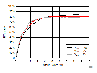
- 84% System Efficiency at 10 W
- WPC v1.2 Compliant Communication and Control for Compatibility With Current TX Solutions
- Patented Transmitter Pad Detect Function Improves User Experience
- Power Signal Frequency Measurement Allows Host to Determine Optimal Placement on TX Surface
- I2C Communication With Host
2 Applications
3 Description
The bq51025 device is a fully-contained wireless power receiver capable of operating in the Wireless Power Consortium (WPC) Qi protocol, which allows a wireless power system to deliver 5 W to the system with Qi inductive transmitters and up to 10 W when operating with the bq500215 primary-side controller. The bq51025 device provides a single device power conversion (rectification and regulation) as well as the digital control and communication as per WPC v1.2 specification. With market-leading 84% system efficiency and adjustable output voltage, the bq51025 device allows for unparalleled system optimization. With a maximum output voltage of 10 V, the bq51025 offers a flexible solution that offers a wireless power solution for 2S battery application and allows optimal thermal performance of the system. The I2C interface allows system designers to implement new features such as aligning a receiver on the transmitter surface or detecting foreign objects on the receiver. The bq51025 device complies with the WPC v1.2 communication protocol making it compatible with all WPC transmitter solutions. The receiver allows for synchronous rectification, regulation and control, and communication to all exist in a market-leading form factor, efficiency, and solution size.
Device Information(1)
| PART NUMBER | PACKAGE | BODY SIZE (NOM) |
|---|---|---|
| bq51025 | DSBGA (42) | 3.60 mm × 2.89 mm |
- For all available packages, see the orderable addendum at the end of the data sheet.
spacer
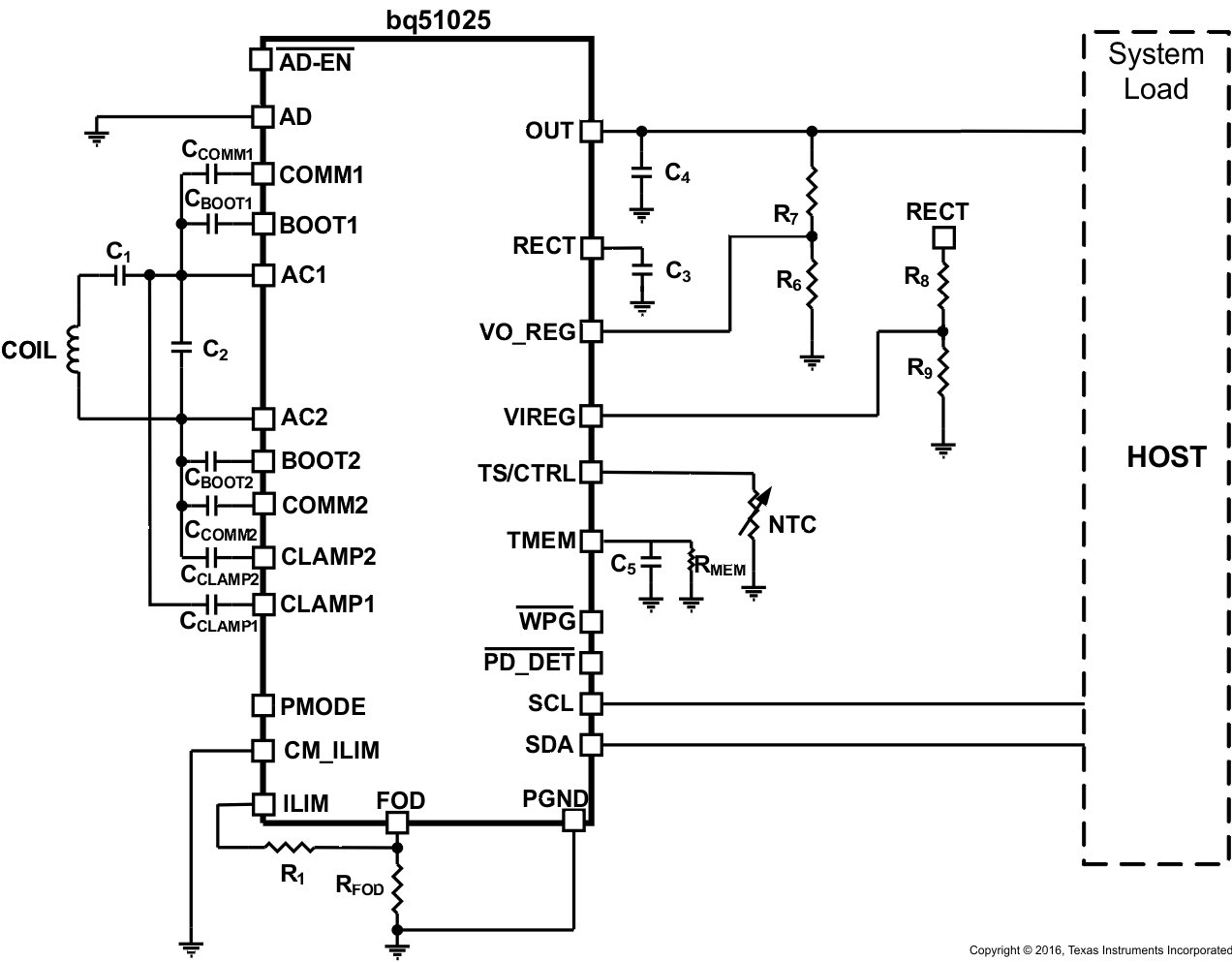
Simplified Schematic

bq51025 System Efficiency With bq500215 TX Controller
