SLUSBX7C September 2014 – March 2017
PRODUCTION DATA.
- 1 Features
- 2 Applications
- 3 Description
- 4 Revision History
- 5 Device Comparison Table
- 6 Pin Configuration and Functions
- 7 Specifications
-
8 Detailed Description
- 8.1 Overview
- 8.2 Functional Block Diagram
- 8.3
Feature Description
- 8.3.1 Dynamic Rectifier Control
- 8.3.2 Dynamic Power Scaling
- 8.3.3 VO_REG Calculations
- 8.3.4 RILIM Calculations
- 8.3.5 Adapter Enable Functionality
- 8.3.6 Turning Off the Transmitter
- 8.3.7 Communication Current Limit
- 8.3.8 PD_DET and TMEM
- 8.3.9 TS/CTRL
- 8.3.10 PMODE Pin
- 8.3.11 I2C Communication
- 8.3.12 Input Overvoltage
- 8.3.13 Alignment Aid Using Frequency Information
- 8.4 Device Functional Modes
- 8.5
Register Maps
- 8.5.1 Wireless Power Supply Current Register 1
- 8.5.2 Wireless Power Supply Current Register 2
- 8.5.3 Wireless Power Supply Current Register 3
- 8.5.4 I2C Mailbox Register
- 8.5.5 I2C Mailbox Register 2
- 8.5.6 I2C Mailbox Register 3
- 8.5.7 Wireless Power Supply FOD RAM
- 8.5.8 Wireless Power User Header RAM
- 8.5.9 Wireless Power USER VRECT Status RAM
- 8.5.10 Wireless Power VOUT Status RAM
- 8.5.11 Wireless Power Proprietary Mode REC PWR MSByte Status RAM
- 8.5.12 Wireless Power REC PWR LSByte Status RAM
- 8.5.13 Wireless Power Prop Packet Payload RAM Byte 0
- 8.5.14 Wireless Power Prop Packet Payload RAM Byte 1
- 8.5.15 Wireless Power Prop Packet Payload RAM Byte 2
- 8.5.16 Wireless Power Prop Packet Payload RAM Byte 3
-
9 Application and Implementation
- 9.1 Application Information
- 9.2
Typical Applications
- 9.2.1
WPC v1.2 Power Supply 7-V Output With 1.4-A Maximum Current With I2C
- 9.2.1.1 Design Requirements
- 9.2.1.2
Detailed Design Procedure
- 9.2.1.2.1 Output Voltage Set Point
- 9.2.1.2.2 Output and Rectifier Capacitors
- 9.2.1.2.3 TMEM
- 9.2.1.2.4 Maximum Output Current Set Point
- 9.2.1.2.5 I2C
- 9.2.1.2.6 Communication Current Limit
- 9.2.1.2.7 Receiver Coil
- 9.2.1.2.8 Series and Parallel Resonant Capacitors
- 9.2.1.2.9 Communication, Boot, and Clamp Capacitors
- 9.2.1.3 Application Curves
- 9.2.2 Standalone 10-V WPC v1.2 Power Supply With 1-A Maximum Output Current in System Board
- 9.2.3
Standalone 10-V Power Supply With 1-A Maximum Output Current for 2S Charging System
- 9.2.3.1 Design Requirements
- 9.2.3.2
Detailed Design Procedure
- 9.2.3.2.1 Output Voltage Set Point
- 9.2.3.2.2 Output and Rectifier Capacitors
- 9.2.3.2.3 TMEM
- 9.2.3.2.4 Maximum Output Current Set Point
- 9.2.3.2.5 I2C
- 9.2.3.2.6 Communication Current Limit
- 9.2.3.2.7 Receiver Coil
- 9.2.3.2.8 Series Resonant Capacitors
- 9.2.3.2.9 Communication, Boot, and Clamp Capacitors
- 9.2.3.2.10 VRECT Clamp
- 9.2.3.3 Application Curves
- 9.2.1
WPC v1.2 Power Supply 7-V Output With 1.4-A Maximum Current With I2C
- 10Power Supply Recommendations
- 11Layout
- 12Device and Documentation Support
- 13Mechanical, Packaging, and Orderable Information
Package Options
Mechanical Data (Package|Pins)
- YFP|42
Thermal pad, mechanical data (Package|Pins)
Orderable Information
9 Application and Implementation
NOTE
Information in the following applications sections is not part of the TI component specification, and TI does not warrant its accuracy or completeness. TI’s customers are responsible for determining suitability of components for their purposes. Customers should validate and test their design implementation to confirm system functionality.
9.1 Application Information
The bq51025 device complies with WPC v1.2 standard. There are several tools available for the design of the system. Obtain these tools by checking the product page at www.ti.com. The following sections detail how to design a WPC v1.2 mode RX system.
9.2 Typical Applications
9.2.1 WPC v1.2 Power Supply 7-V Output With 1.4-A Maximum Current With I2C
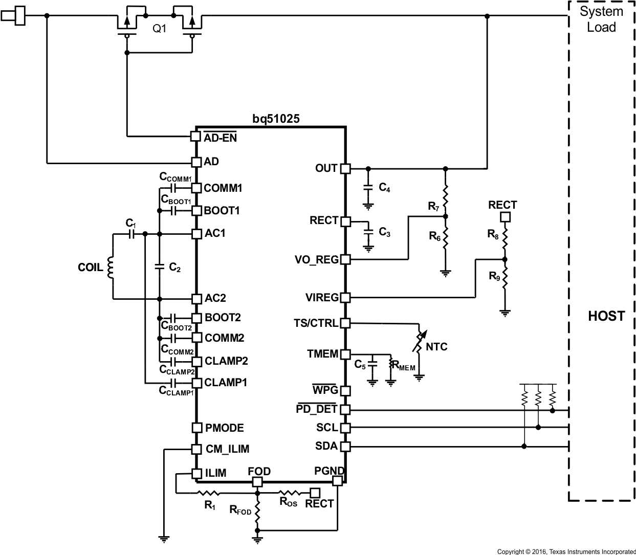 Figure 14. Schematic Using bq51025
9.2.1.1 Design Requirements
Table 20 shows the design parameters.
Table 20. Design Parameters
| DESIGN PARAMETER | EXAMPLE VALUE |
|---|---|
| VOUT | 7 V |
| IOUT MAXIMUM | 1.4 A |
9.2.1.2 Detailed Design Procedure
To start the design procedure, determine the following:
- Output voltage
- Maximum output current
9.2.1.2.1 Output Voltage Set Point
The output voltage of the bq51025 device can be set by adjusting a feedback resistor divider network. The resistor divider network is used to set the voltage gain at the VO_REG pin. The device is intended to operate where the voltage at the VO_REG pin is set to 0.5 V. This value is the default setting and can be changed through I2C. In Figure 15, R6 and R7 are the feedback network for the output voltage sense.
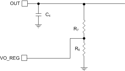 Figure 15. Voltage Gain for Feedback


Choose R7 to be a standard value. In this case, take care to choose R6 and R7 to be fairly large values so as to not dissipate an excessive amount of power in the resistors and thereby lower efficiency.
KVO is set to be 0.5 / 7 = 1/14, choose R7 to be 130 kΩ, and thus R6 to be 10 kΩ.
After R6 and R7 are chosen, the same values should be used on the VI_REG resistor divider (R9 and R8). This allows the device to regulate the rectifier voltage properly and accurately track the output voltage.
9.2.1.2.2 Output and Rectifier Capacitors
Set C4 between 1 and 4.7 µF. This example uses 3.3 µF.
Set C3 between 22 and 44 µF. This example uses 44 µF to minimize output ripple.
9.2.1.2.3 TMEM
Set C5 to 2.2 µF. To determine the bleedoff resistor, the WPC transmitters (for which the PD_DET is being set for) needs to be determined. After the ping timing (time between two consecutive digital pings after EPT charge complete is sent) is determined, the bleedoff resistor RMEM can be determined. This example uses TI transmitter EVMs as the use case. In this case, the time between pings is 5 s. To set the time constant using Equation 9, RMEM is set to 560 kΩ.
9.2.1.2.4 Maximum Output Current Set Point
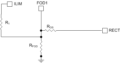 Figure 16. Current Limit Setting for bq51025
The bq51025 device includes a means of providing hardware overcurrent protection by means of an analog current regulation loop. The hardware current limit provides a level of safety by clamping the maximum allowable output current (for example, a current compliance). The RILIM resistor size also sets the thresholds for the dynamic rectifier levels, and thus providing efficiency tuning per each application’s maximum system current. The calculation for the total RILIM resistance is as follows:


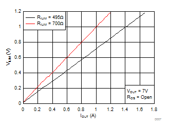
The RILIM allows for the ILIM pin to reach 1.2 V at an output current equal to IILIM in 10-W mode and reach 0.6 V in 5-W mode. When choosing IILIM, consider two possible operating conditions:
- If the application requires an output current equal to or greater than external ILIM that the circuit is designed for (input current limit on the charger where the RX is delivering power to is higher than the external ILIM), ensure that the downstream charger is capable of regulating the voltage of the input into which the RX device output is tied to by lowering the amount of current being drawn. This ensures that the RX output does not collapse. Such behavior is referred to as VIN DPM in TI chargers. Unless such behavior is enabled on the charger, the charger pulls the output of the RX device to ground when the RX device enters current regulation.
- If the applications are designed to extract less than the IMAX, typical designs should leave a design margin of at least 20% so that the voltage at ILIM pin reaches 1.2 V when 20% more than maximum current of the system (IMAX) is drawn from the output of the RX. Such a design would have input current limit on the charger lower than the external current limit of the RX device.
In both cases, however, the charger must be capable of regulating the current drawn from the device to allow the output voltage to stay at a reasonable value. This same behavior is also necessary during the WPC v1.2 Communication. See Communication Current Limit for more details. The following calculations show how such a design is achieved:


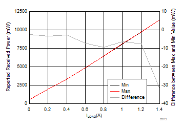
When referring to the application diagram shown in Figure 16, RILIM is the sum of the R1 and RFOD resistance (that is, the total resistance from the ILIM pin to GND). RFOD is chosen according to the FOD application note that can be obtained by contacting your TI representative. This is used to allow the RX implementation to comply with WPC v1.2 requirements related to received power accuracy.
Also note that in many applications, the resistor ROS is necessary to comply with WPC v1.2 requirements. In such a case, the offset on the FOD pin from the voltage on RFOD can cause a shift in the calculation that can reduce the expected current limit. Therefore, it is always a good idea to check the output current limit after FOD calibration is performed according to the FOD section. Unfortunately, because the RECT voltage is not deterministic, and depends on transmitter operation to a certain degree, it is not possible to determine R1 with ROS present in a deterministic manner.
In this example, set maximum current for the example to be 1.4 A at 10 W and 700 mA at 5-W mode. Set IILIM = 1.7 A to allow for the 20% margin.

9.2.1.2.5 I2C
The I2C lines are used to communicate with the device. To enable the I2C, they can be pulled up to an internal host bus. The device address is 0x6C.
9.2.1.2.6 Communication Current Limit
Communication current limit allows the device to communicate with the transmitter in an error-free manner by decoupling the coil from load transients on the OUT pin during WPC communication. In some cases, this communication current limit feature is not desirable. In this design, the user enables the communication current limit by tying the CM_ILIM pin to GND. If this is not needed, the CM_ILIM pin can be tied to the OUT pin to disable the communication current limit. In this case, take care that the voltage on the CM_ILIM pin does not exceed the maximum rating of the pin.
9.2.1.2.7 Receiver Coil
The receiver coil design is the most open part of the system design. The choice of the receiver inductance, shape, and materials all intimately influence the parameters themselves in an intertwined manner. This design can be complicated and involves optimizing many different aspects; refer to the EVM user's guide (SLUUB55).
The typical choice of the inductance of the receiver coil for a 10-W, 7-V solution is between 15 and 16 µH.
9.2.1.2.8 Series and Parallel Resonant Capacitors
Resonant capacitors, C1 and C2, are set according to WPC specification.
The equations for calculating the values of the resonant capacitors are shown:
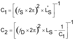
Because the bq51025 can provide up to 10 W of output power, TI highly recommends that the resonant capacitors have very-low ESR and dissipate as little power as possible for better thermal performance. TI highly recommends NP0/C0G ceramic material capacitors.
9.2.1.2.9 Communication, Boot, and Clamp Capacitors
Set CCOMMx to a value ranging from C1 / 8 to C1 / 3. The higher the value of the communication capacitors, the easier it is to comply with the WPC specification. However, higher capacitors do lower the overall efficiency of the system. Make sure these are X7R ceramic material and have a minimum voltage rating of 25 V.
Set CBOOTx as 15 nF. Make sure these are X7R ceramic material and have a minimum voltage rating of 25 V.
Set CCLAMPx as 470 nF. Make sure these are X7R ceramic material and have a minimum voltage rating of 25 V.
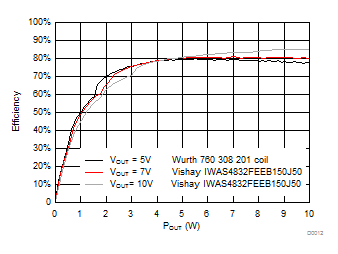
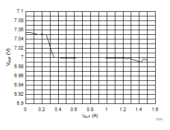
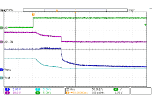
9.2.1.3 Application Curves
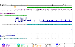
| CM_ILIM = High | CH1 = VRECT | CH2 = VOUT |
| CH3 = PMODE | CH4 = ILOAD |
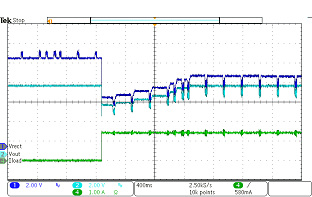
| CM_ILIM = High | CH1 = VRECT | CH2 = VOUT |
| CH4 = ILOAD |
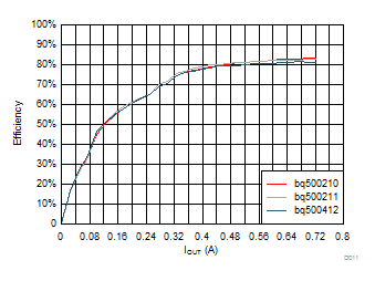
| CM_ILIM = High | ||
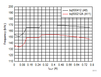
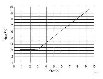
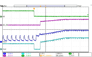
| CH1 = VRECT | CH2 = VOUT | |
| CH3 = AD_EN | CH4 = AD | |
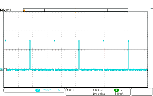
| CH2 = VTS | ||
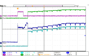
| CM_ILIM = High | CH1 = VRECT | CH2 = VOUT |
| CH3 = PMODE | CH4 = ILOAD |
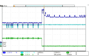
| CM_ILIM = High | CH1 = VRECT | CH2 = VOUT |
| CH4 = ILOAD |
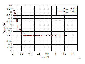
| CM_ILIM = High | ||
| CH1 = VRECT | CH2 = VOUT | |
| CH3 = AD_EN | CH4 = AD | |
9.2.2 Standalone 10-V WPC v1.2 Power Supply With 1-A Maximum Output Current in System Board
When the bq5102x device is implemented as an embedded device on the system board, the same design procedure as for an I2C system should be used, but the I2C pins are to be connected to ground.The VO_REG and VIREG resistor dividers are chosen to achieve 10-V output and RILIM is chosen to allow a maximum current of 1 A (IILIM = 1.2 A for 20% margin). Refer to WPC v1.2 Power Supply 7-V Output With 1.4-A Maximum Current With I2C for details on how these resistor values are calculated.
A typical coil inductance for 10-V is between 15 and 17 µH. It is important to note that even if the same receiver coil and tuning as for a 7-V RX solution are used (see Receiver Coil and Series and Parallel Resonant Capacitors), the RFOD and ROS values need to be updated to accurately determine the received power.
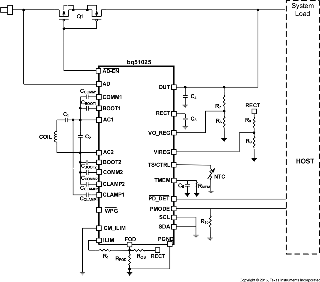 Figure 32. bq51025 Embedded in a System Board
9.2.3 Standalone 10-V Power Supply With 1-A Maximum Output Current for 2S Charging System
For the bq51025 to work properly as a supply to a 2S charger, the bq51025 output voltage must not drop below the minimum input charging voltage of the charger, which may be around 9 V depending on the charger IC. In a WPC tuned Rx/TX system, the power delivered to the load may change during Rx/Tx communication due to the capacitive modulation when CCOMM1 and CCOMM2 are connected form AC1 and AC2 pins to ground. If the power delivered to the load decreases, the VRECT voltage will drop and so may VOUT. if the charger IC does not have input DPM. If the power delivered to the load does not change or increases for a given current, the VRECT voltage will increase and the bq51025 will regulate the voltage.
NOTE
The following design example is for a 2S charging system where the charger IC does not have input DPM feature.
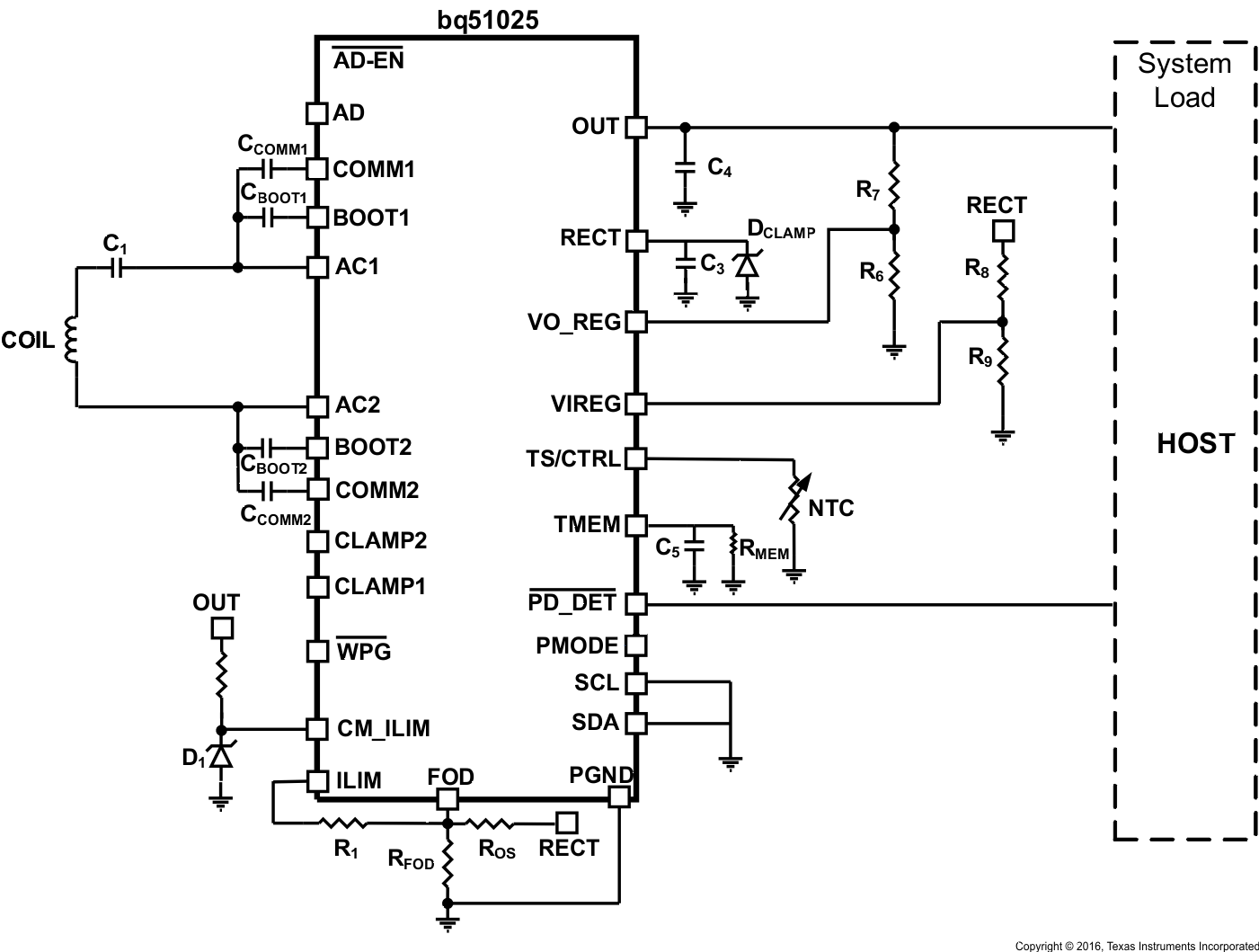 Figure 33. bq51025 Embedded in a 2S Battery System Board
9.2.3.1 Design Requirements
Table 21 shows the design parameters.
Table 21. Design Parameters
| DESIGN PARAMETER | EXAMPLE VALUE |
|---|---|
| VOUT | 10 V |
| IOUT MAXIMUM | 1 A |
9.2.3.2 Detailed Design Procedure
To start the design procedure, determine the following:
- Output voltage
- Maximum output current
9.2.3.2.1 Output Voltage Set Point
The output voltage of the bq51025 device can be set by adjusting a feedback resistor divider network as described in Output Voltage Set Point. The ratio of VO_REG and VIREG resistor dividers are chosen to achieve 10-V based on the 0.5-V feedback voltage. Following Equation 12 and Equation 13, R6 and R7 are selected to be 11.3KΩ- and 215-kΩ, respectively. The same values are used on R9 and R8 in the VIREG divider.
9.2.3.2.2 Output and Rectifier Capacitors
Set C4 to at least 3.3 µF.
Set C3 to at least 44 µF to minimize output ripple. Use capacitors rated for 25 V or higher.
9.2.3.2.3 TMEM
Follow procedure described in TMEM.
9.2.3.2.4 Maximum Output Current Set Point
Follow the procedure described in Maximum Output Current Set Point.
9.2.3.2.5 I2C
Connect I2C lines to ground.
9.2.3.2.6 Communication Current Limit
Communication current limit must be disabled. Connect CM_ILIM pin to voltage supply making sure it does not exceed maximum absolute rating for the pin. If only the battery voltage is available, use a 5-V Zener diode (D1) to clamp the voltage.
9.2.3.2.7 Receiver Coil
The receiver coil design is the most open part of the system design. The choice of the receiver inductance, shape, and materials all intimately influence the parameters themselves in an intertwined manner. This design can be complicated and involves optimizing many different aspects. The typical choice of the inductance of the receiver coil for a 10-W, 10-V solution is between 15 and 16 µH.
9.2.3.2.8 Series Resonant Capacitors
In order for the bq51025 to work properly as a supply to a 2S charger, the bq51025 output voltage must not drop below the minimum input charging voltage of the charger, which may be around 9 V depending on the charger IC. In a WPC tuned Rx/Tx system, the power delivered to the load may change during Rx/Tx communication due to the capacitive modulation when CCOMM1 and CCOMM2 are connected from AC1 and AC2 pins to ground. If the power delivered to the load decreases, the VRECT voltage will drop and so may VOUT if the charger IC does not have VIN-DPM function. If the power delivered to the load does not change or increases for a given current, the VRECT voltage will increase and the bq51025 will regulate the voltage to a fixed value. The following section discusses the tuning procedure to ensure that the output voltage level is maintained during communication when operating with a bq51025 based transmitter.
9.2.3.2.8.1 Tuning Procedure
NOTE
The following tuning procedure results in a system that is not compliant with WPC specification and is only designed to operate with a given bq500215 based transmitter.
- Measure the effective self-inductance of the bq500215 based transmitter (primary) coil, LP' , and receiver (secondary) coil, LS'. The measurements must be done on the final charging system setup (that is, battery and any other friendly metal of the device is included as well as any cover material that determines the distance between the coil and charging surface). Make the measurement at the optimal alignment position.
- Measure the mutual inductance, LM and calculate the coupling factor given by:
- A first-order approximation of the series capacitance is given by:
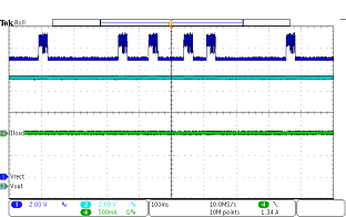
- Make sure C1 as well as CCOMM1 and CCOMM2 are populated and place the receiver with best possible alignment on the transmitter and start power transfer. Using an oscilloscope, monitor the VRECT voltage during communication at maximum load. If VRECT decreases during communication, increase C1 until the voltage remains flat. Note that the larger the VRECT voltage increase is during communication at maximum load, the larger the losses on the device. The voltage increase in VRECT is larger with lower load and lower coupling, so it is important to keep the VRECT voltage as low as possible during communication at maximum load and coupling to maximize efficiency across charging area and load range. Figure 35 and Figure 36 show how the VRECT voltage behavior after tuning
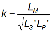

Where f is the operating frequency of the transmitter, which is 130 kHz and CP is the transmitter resonant capacitance which is 247 nF.
9.2.3.2.9 Communication, Boot, and Clamp Capacitors
Set CCOMMx to a value ranging from C1 / 8 to C1 / 3. Make sure these are X7R ceramic material and have a minimum voltage rating of 25 V. For this example 56-nF capacitors are chosen.
Set CBOOTx as 15 nF. Make sure these are X7R ceramic material and have a minimum voltage rating of 25 V.
CCLAMPx is not populated since a external clamping diode is used.
9.2.3.2.10 VRECT Clamp
Connect a 12-V Zener diode (DCLAMP) from VRECT to ground. This diode prevents the rectifier voltage from overshoot above VRECT-OVP level, preventing unwanted resets during large load transients during communication.
9.2.3.3 Application Curves

| CH1 = VRECT | CH2 = VOUT | |
| CH4 = ILOAD |
| CH1 = VRECT | CH2 = VOUT | |
| CH4 = ILOAD |
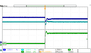
| CH1 = VRECT | CH2 = VOUT | |
| CH4 = ILOAD | ||
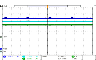
| CH1 = VRECT | CH2 = VOUT | |
| CH4 = ILOAD |
With 1-A Load
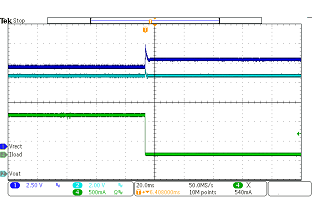
| CH1 = VRECT | CH2 = VOUT | |
| CH4 = ILOAD |
With 10-V Tuned RX
