SLUSBS9A February 2014 – July 2014
PRODUCTION DATA.
- 1 Features
- 2 Applications
- 3 Description
- 4 Simplified Schematic
- 5 Revision History
- 6 Device Comparison Table
- 7 Pin Configuration and Functions
- 8 Specifications
-
9 Detailed Description
- 9.1 Overview
- 9.2 Functional Block Diagram
- 9.3
Feature Description
- 9.3.1 Dynamic Rectifier Control
- 9.3.2 Dynamic Power Scaling
- 9.3.3 VO_REG and VIREG Calculations
- 9.3.4 RILIM Calculations
- 9.3.5 Adapter Enable Functionality
- 9.3.6 Turning Off the Transmitter
- 9.3.7 CM_ILIM
- 9.3.8 PD_DET and TMEM
- 9.3.9 TS, Both WPC and PMA
- 9.3.10 I2C Communication
- 9.3.11 Input Overvoltage
- 9.4 Device Functional Modes
- 9.5 Register Maps
-
10Application and Implementation
- 10.1 Application Information
- 10.2
Typical Applications
- 10.2.1
Dual Mode Design (WPC and PMA Compliant) Power Supply 5-V Output With 1-A Maximum Current
- 10.2.1.1 Design Requirements
- 10.2.1.2
Detailed Design Procedure
- 10.2.1.2.1 Output Voltage Set Point
- 10.2.1.2.2 Output and Rectifier Capacitors
- 10.2.1.2.3 Maximum Output Current Set Point
- 10.2.1.2.4 TERM Resistor
- 10.2.1.2.5 Setting LPRB1 and LPRB2 Resistors
- 10.2.1.2.6 I2C
- 10.2.1.2.7 Communication Current Limit
- 10.2.1.2.8 Receiver Coil
- 10.2.1.2.9 Series and Parallel Resonant Capacitors
- 10.2.1.2.10 Communication, Boot and Clamp Capacitors
- 10.2.1.3 Application Curves
- 10.2.2 bq51221 Embedded in System Board
- 10.2.3 bq51221 Implemented in Back Cover
- 10.2.1
Dual Mode Design (WPC and PMA Compliant) Power Supply 5-V Output With 1-A Maximum Current
- 11Power Supply Recommendations
- 12Layout
- 13Device and Documentation Support
- 14Mechanical, Packaging, and Orderable Information
Package Options
Mechanical Data (Package|Pins)
- YFP|42
Thermal pad, mechanical data (Package|Pins)
Orderable Information
10 Application and Implementation
10.1 Application Information
The bq51221 device is a dual mode device which complies with both WPC v1.1 and PMA standards. This allows a system designer to design a system that complies with both wireless power standards. There are several tools available for the design of the system. These tools may be obtained by checking the product page at www.ti.com/product/bq51221. The following sections detail how to design a dual mode RX system.
10.2 Typical Applications
10.2.1 Dual Mode Design (WPC and PMA Compliant) Power Supply 5-V Output With 1-A Maximum Current
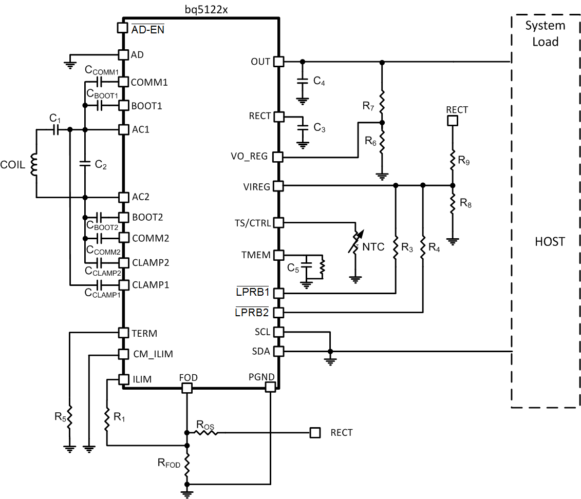 Figure 16. Dual Mode Schematic Using bq51221
10.2.1.1 Design Requirements
Table 19. Design Parameters
| DESIGN PARAMETER | EXAMPLE VALUE |
|---|---|
| VOUT | 5 V |
| IOUT MAXIMUM | 1 A |
| MODE | WPC and PMA |
10.2.1.2 Detailed Design Procedure
To start the design procedure, start by determining the following.
- Mode of operation – in this case dual mode (WPC and PMA)
- Output voltage
- Maximum output current
10.2.1.2.1 Output Voltage Set Point
The output voltage of the bq51221 device can be set by adjusting a feedback resistor divider network. The resistor divider network is used to set the voltage gain at the VO_REG pin. The device is intended to operate where the voltage at the VO_REG pin is set to 0.5 V. This value is the default setting and can be changed through I2C. In Figure 17, R6 and R7 are the feedback network for the output voltage sense.
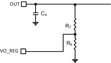 Figure 17. Voltage Gain for Feedback


Choose R7 to be a standard value. In this case, care should be taken to choose R6 and R7 to be fairly large values so as to not dissipate excessive amount of power in the resistors and thereby lower efficiency.
KVO is set to be 0.5 / 5 = 0.1, choose R7 to be 102 kΩ, and thus R6 to be 11.3 kΩ.
After R6 and R7 are chosen, the same values should be used on R8 and R9. This allows the device to regulate the rectifier in the PMA mode to accurately track the output voltage when the output voltage is changed through I2C.
10.2.1.2.2 Output and Rectifier Capacitors
Set C4 between 1 µF and 4.7 µF. This example uses 1 µF.
Set C3 between 4.7 µF and 22 µF. This example uses 20 µF.
10.2.1.2.2.1 TMEM
Set C5 to 2.2 µF. In order to determine the bleed off resistor, the WPC transmitters for which the PD_DET is being set for needs to be determined. After the ping timing (time between two consecutive digital pings after EPT charge complete is sent) is determined, the bleedoff resistor can be determined. This example uses TI transmitter EVMs as the use case. In this case the time between pings is 5 s. In order to set the time constant using Equation 8, it is set to 560 kΩ.
10.2.1.2.3 Maximum Output Current Set Point
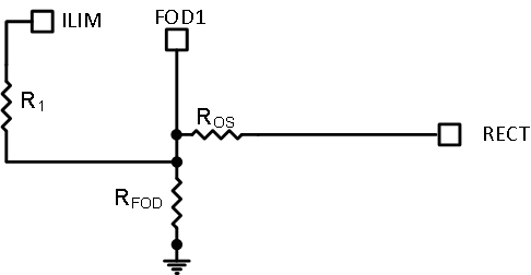 Figure 18. Current Limit Setting for bq51221
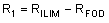
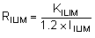
The bq51221 device includes a means of providing hardware overcurrent protection by means of an analog current regulation loop. The hardware current limit provides a level of safety by clamping the maximum allowable output current (for example, a current compliance). The RILIM resistor size also sets the thresholds for the dynamic rectifier levels and thus providing efficiency tuning per each application’s maximum system current. The calculation for the total RILIM resistance is as follows:

The RILIM will allow for the ILIM pin to reach 1.2 V at an output current equal to IILIM. When choosing RILIM, two options are possible.
If the application requires an output current equal to or greater than external ILIM that the circuit is designed for (input current limit on the charger where the RX is delivering power to is higher than the external ILIM), ensure that the downstream charger is capable of regulating the voltage of the input into which the RX device output is tied to by lowering the amount of current being drawn. This will ensure that the RX output does not collapse.
Such behavior is referred to as VIN-DPM in TI chargers. Unless such behavior is enabled on the charger, the charger will pull the output of the RX device to ground when the RX device enters current regulation.
If the applications are designed to extract less than the ILIM (1-A maximum), typical designs should leave a design margin of at least 20% so that the voltage at ILIM pin reaches 1.2 V when 20% more than maximum current of the system is drawn from the output of the RX. Such a design would have input current limit on the charger lower than the external ILIM of the RX device.
In both cases however, the charger must be capable of regulating the current drawn from the device to allow the output voltage to stay at a reasonable value. This same behavior is also necessary during the WPC V1.1 Communication. See Communication Current Limit for more details. The following calculations show how such a design is achieved:
When referring to the application diagram shown in Figure 18, RILIM is the sum of the R1 and RFOD resistance (that is, the total resistance from the ILIM pin to GND). RFOD is chosen according to the FOD application note that can be obtained by contacting your TI representative. This is used to allow the RX implementation to comply with WPC v1.1 requirements related to received power accuracy.
Also note that in many applications, the resistor ROS is needed in order to comply with WPC V1.1 requirements. In such a case, the offset on the FOD pin from the voltage on RFOD can cause a shift in the calculation that can reduce the expected current limit. Therefore, it is always a good idea to check the output current limit after FOD calibration is performed according to the FOD section shown below. Unfortunately, because the RECT voltage is not deterministic, and depends on transmitter operation to a certain degree, it is not possible to determine R1 with ROS present in a deterministic manner.
In this example, set maximum current for the example to be 1000 mA. To set IILIM = 1.2 A to allow for the 20% margin.

10.2.1.2.4 TERM Resistor
The TERM resistor is used to set the termination threshold on the RX. The device will send an EPT Charge Complete, or EOC message to the transmitter and thus allow for the system to go into a low standby mode. This is also mandated through PMA specification.
By picking a resistor to ground from the TERM pin the system designer can set the termination threshold. The device will send the EPT/EOC message, when the voltage on the ILIM pin goes below the voltage on the TERM pin. The designer can therefore set a resistor on the TERM pin that will determine the threshold.
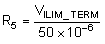
Typically, one can use RILIM to set R5 resistor such that at the desired current, on OUT pin, VILIM_TERM can be reached. However, this can be made indeterministic because of the presence of the Ros resistor that is used to comply with WPC v1.1 FOD requirements. Therefore, the system designer is suggested to measure the voltage on the ILIM pin at the output current where he would like to set the termination. This voltage on the ILIM pin is termed as VILIM_TERM. In the design example, to set 50 mA, measure VILIM_TERM. After this is done, set the resistor R5 using the equation Equation 17.
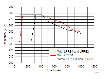
10.2.1.2.5 Setting LPRB1 and LPRB2 Resistors
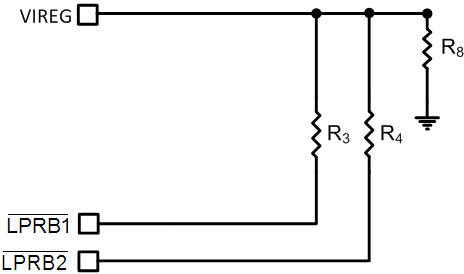 Figure 19. Setting Low Power Rectifier Boost
LPRB1 and LPRB2 are multifunction pins. Depending on whether the termination resistor is used or not, the LPRB pins will change function. This allows the designer to optimize the PMA design for efficiency or transient performance.
Table 20. LPRB Setup for Different Applications
| Implementation | TERM Resistor | Ball Number F5 | Ball Number G6 |
|---|---|---|---|
| Backcover | Populated | LPRB1 | LPRB2 |
| Embedded | Not populated | WPG | PD_DET |
For more information on how to set the TERM resistor, see TERM Resistor.
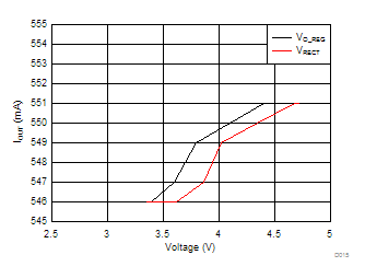
The LPRBx boosts the rectifier voltage to a higher voltage, and thus it sets the transmitter in PMA mode to operate in frequency or load line that can sustain load step which is part of the PMA certification process. LPRB1 is used to boost the rectifier voltage at low power (output current below about 95 mA). LPRB2 is used to boost the rectifier voltage when output current is below about 310 mA). Both pins are connected to VIREG through resistors, R3 and R4 as shown in Setting LPRB1 and LPRB2 Resistors. These two values depend on the coil and the output voltage choice. Also, the allowable voltage drop also defined by the board manufacturer can allow you to set the voltage in these modes to optimize the efficiency and transient response. To design R3 and R4, set a window of VRECT to boost the operating frequency of the TX a 0-mA load and 100 mA
Good starting points are: 7.3 to 7.8 V for 0 to 100 mA and 6.7 to 7.3 V for 100 to 400 mA
Now, find the values of R3 and R4 that can provide the chosen window. The lower and upper reference of VIREG is 0.4906 and 0.5318 V
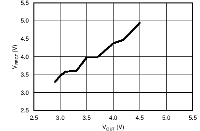
Calculate VRECT as follows using the TI tool provided in the product folder under the "Tools & sofware" tab.
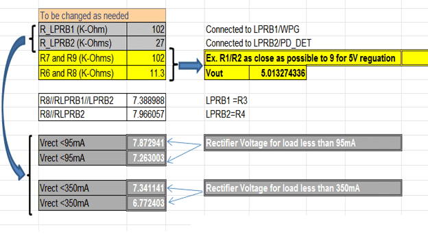 Figure 20. LPRB Resistor Calculations
10.2.1.2.6 I2C
The I2C lines are used to communicate with the device. In order to enable the I2C, they can be pulled up to an internal host bus. When not in use as in Figure 41, tie them to GND. The device address is 0x6C.
10.2.1.2.7 Communication Current Limit
Communication current limit allows the device to communicate with the transmitter in an error free manner by decoupling the coil from load transients on the OUT pin during WPC communication. In some cases this communication current limit feature is not desirable. In this design, the user enables the communication current limit. This is done by tying the CM_ILIM pin to GND. In the case that this is not needed, the CM_ILIM pin can be tied to OUT pin to disable the communication current limit. In this case, take care that the voltage on the CM_ILIM pin does not exceed the maximum rating of the pin.
10.2.1.2.8 Receiver Coil
The receiver coil design is the most open and interesting part of the system design. The choice of the receiver inductance, shape, and materials all intimately influence the parameters themselves in an intertwined manner. This design can be complicated and involves optimizing many different aspects; refer to the user's guide for the EVM (SLUUAX6).
The typical choice of the inductance of the receiver coil for a dual mode 5-V solution is between 6 to 8 µH.
10.2.1.2.9 Series and Parallel Resonant Capacitors
Resonant capacitors C1 and C2 are set according to WPC specification. Although this is a dual mode solution, the PMA does not specify an exact resonance frequency for the resonant capacitors and in fact does not specify that resonant capacitors are indeed needed.
The equations for calculating the values of the resonant capacitors are shown:
10.2.1.2.10 Communication, Boot and Clamp Capacitors
Set CCOMMx to a value ranging from C1 / 8 to C1 / 3. The higher the value of the communication capacitors, the easier it is to comply with PMA specification. However, higher capacitors do lower the overall efficiency of the system. Make sure these are X7R ceramic material and have a minimum voltage rating of 25 V.
Set CBOOTx to be 15 nF. Make sure these are X7R ceramic material and have a minimum voltage rating of 25 V.
Set CCLAMPx to be 470 nF. Make sure these are X7R ceramic material and have a minimum voltage rating of
25 V.
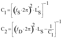
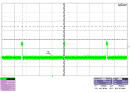
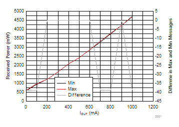
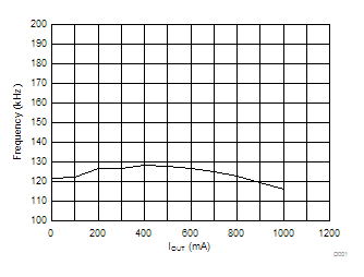
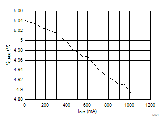
10.2.1.3 Application Curves
| Ch1: VOUT, 1 V | Ch3: unused | 400 ms/Div |
| Ch2: VRECT, 1 V | Ch4: IOUT, 200 mA | |
| Ch1: VOUT, 1 V | Ch3: unused | 2 ms/Div |
| Ch2: VRECT, 1 V | Ch4: unused | |
| Ch1: TS, 1 V | Ch3: unused | 400 ms/Div |
| Ch2: unused | Ch4: unused | |
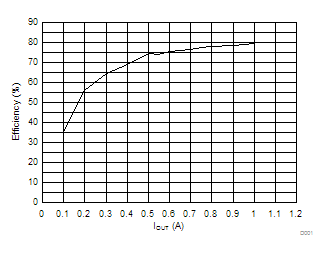
| VOUT = 5 V | ||
| RILIM = 700 Ω | ||
| TX: bq500210EVM-689, RX: bq51221EVM-520 | ||
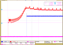
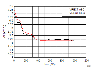
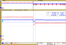
| Ch1: unused | Ch3: VRECT, 2 V | 2 ms/Div |
| Ch2: IOUT, 500 mA | Ch4: VOUT, 2 V | |
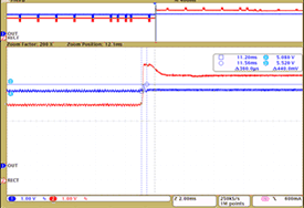
| Ch1: unused | Ch3: unused | 500 ms/Div |
| Ch2: unused | Ch4: TS, 500 mV | |
| PMA mode, operating in current limit | ||
| IILIM = 1 A |
| Ch1: VOUT, 1 V | Ch3: unused | 2 ms/Div |
| Ch2: VRECT, 1 V | Ch4: IOUT, 200 mA | |
| Data taken over approximately 3 minutes | ||
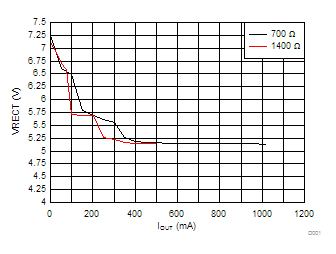
| RILIM = 700 Ω | ||
| RILIM = 1400 Ω |
| VOUT = 5 V | ||
| TX: bq500210EVM-689, RX: bq51221EVM-520 | ||
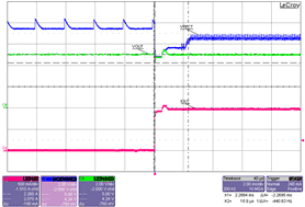
| Ch1: PMA communication, 5 V | Ch3: VRECT, 5 V | 50 ms/Div |
| Ch2: IOUT, 1 A | Ch4: VOUT, 2 V | |
| Ch1: unused | Ch3: VRECT, 2 V | 2 ms/Div |
| Ch2: IOUT, 500 mA | Ch4: VOUT, 2 V | |
| VOUT = 5 V | ||
| TX: Duracell Powermat, RX: bq51221EVM-520 | ||
10.2.2 bq51221 Embedded in System Board
When the bq51221 device is implemented as an embedded device on the system board, LPRBEN (TERM) pin is floated and WPG and PD_DET are set to their function. When LPRBEN has a resistor to ground to enable TERM, PD_DET becomes LPRB1 and WPG becomes LPRB2. This second configuration with TERM enabled is preferred for a back cover implementation. A back cover implementation is one where the receiver device and receiver coil are contained in the back cover of the mobile phone where the receiver is being implemented. With an embedded implementation (one where only the coil is in the mobile device back cover and the receiver device is on the main motherboard for the mobile phone and is controlled by the host controller device in the phone), the expectation is that the host controller (PMIC or Charger) will use the TS/CTRL pin to establish termination and associated EPT or EOC.
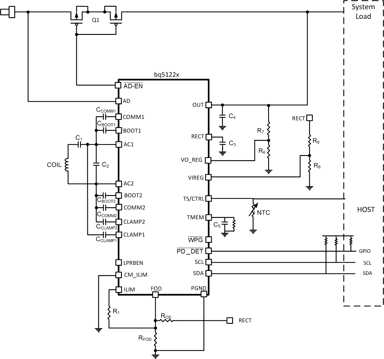 Figure 40. bq51221 Embedded in a System Board
Refer to Dual Mode Design (WPC and PMA Compliant) Power Supply 5-V Output With 1-A Maximum Current for all design details.
10.2.3 bq51221 Implemented in Back Cover
When the bq51221 device is implemented as a back cover solution, set TERM resistor to enable PMA term and LPRB1 and LPRB2 functions are automatically enabled. In this implementation, the bq51221 device can autonomously determine if EOC can be established because the termination current has been reached. In this configuration, PD_DET becomes LPRB1 and WPG becomes LPRB2. This allows the RECT voltage to be controlled at different levels so that transient performance from light load to maximum current can be optimized.
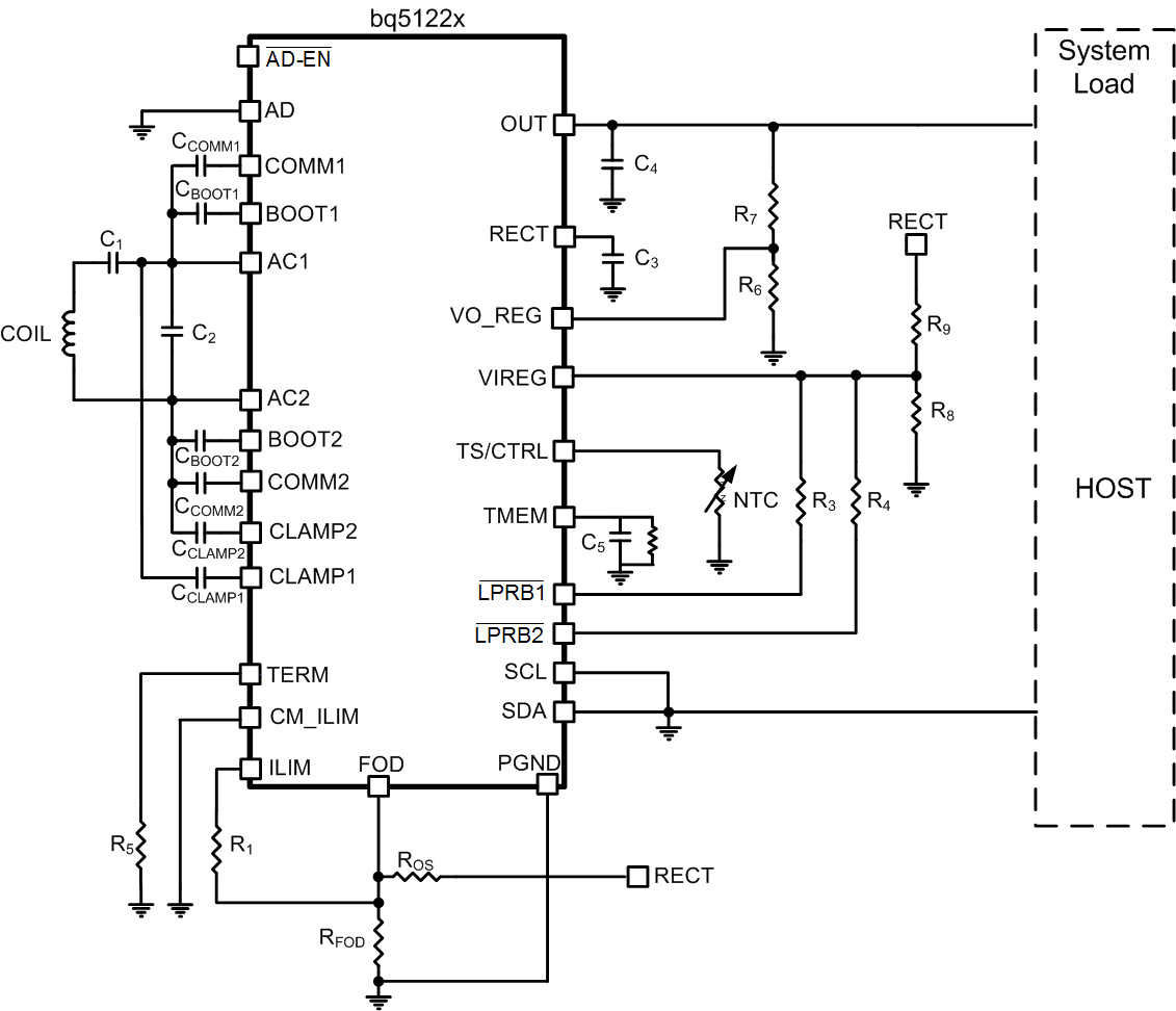 Figure 41. bq51221 Implemented in a Back Cover
Refer to Dual Mode Design (WPC and PMA Compliant) Power Supply 5-V Output With 1-A Maximum Current for all design details.