SLUSAX0E December 2012 – April 2021 BQ7716
PRODUCTION DATA
- 1 Features
- 2 Applications
- 3 Description
- 4 Revision History
- 5 Device Comparison Table
- 6 Pin Configuration and Functions
- 7 Specifications
- 8 Detailed Description
- 9 Application and Implementation
- 10Power Supply Recommendations
- 11Layout
- 12Device and Documentation Support
- 13Mechanical, Packaging, and Orderable Information
Package Options
Mechanical Data (Package|Pins)
- DPJ|8
Thermal pad, mechanical data (Package|Pins)
Orderable Information
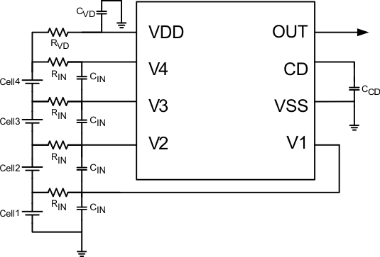
9.1 Application Information
Figure 9-1 shows each external component.
 Figure 9-1 Application Configuration
Note:
In the case of an Open Drain Active Low configuration, an external pull-up resistor is required on the OUT terminal.
Changes to the ranges stated in Table 9-1 will impact the accuracy of the cell measurements.
Note:
The device is calibrated using an RIN value = 1 kΩ. Using a value other than this recommended value changes the accuracy of the cell voltage measurements and VOV trigger level.