SWRS046I November 2006 – September 2018 CC1020
PRODUCTION DATA.
- 1Device Overview
- 2Revision History
- 3Terminal Configuration and Functions
-
4Specifications
- 4.1 Absolute Maximum Ratings
- 4.2 ESD Ratings
- 4.3 Recommended Operating Conditions
- 4.4 RF Transmit
- 4.5 RF Receive
- 4.6 RSSI / Carrier Sense
- 4.7 Intermediate Frequency (IF)
- 4.8 Crystal Oscillator
- 4.9 Frequency Synthesizer
- 4.10 Digital Inputs and Outputs
- 4.11 Current Consumption
- 4.12 Thermal Resistance Characteristics for VQFNP Package
-
5Detailed Description
- 5.1 Overview
- 5.2 Functional Block Diagram
- 5.3 Configuration Overview
- 5.4 Microcontroller Interface
- 5.5 4-wire Serial Configuration Interface
- 5.6 Signal Interface
- 5.7 Data Rate Programming
- 5.8 Frequency Programming
- 5.9
Receiver
- 5.9.1 IF Frequency
- 5.9.2 Receiver Channel Filter Bandwidth
- 5.9.3 Demodulator, Bit Synchronizer, and Data Decision
- 5.9.4 Receiver Sensitivity Versus Data Rate and Frequency Separation
- 5.9.5 RSSI
- 5.9.6 Image Rejection Calibration
- 5.9.7 Blocking and Selectivity
- 5.9.8 Linear IF Chain and AGC Settings
- 5.9.9 AGC Settling
- 5.9.10 Preamble Length and Sync Word
- 5.9.11 Carrier Sense
- 5.9.12 Automatic Power-up Sequencing
- 5.9.13 Automatic Frequency Control
- 5.9.14 Digital FM
- 5.10 Transmitter
- 5.11 Input and Output Matching and Filtering
- 5.12 Frequency Synthesizer
- 5.13 VCO and LNA Current Control
- 5.14 Power Management
- 5.15 On-Off Keying (OOK)
- 5.16 Crystal Oscillator
- 5.17 Built-in Test Pattern Generator
- 5.18 Interrupt on Pin DCLK
- 5.19 PA_EN and LNA_EN Digital Output Pins
- 5.20 System Considerations and Guidelines
- 5.21 Antenna Considerations
- 5.22 Configuration Registers
- 6Applications, Implementation, and Layout
- 7Device and Documentation Support
- 8Mechanical Packaging and Orderable Information
Package Options
Mechanical Data (Package|Pins)
- RSS|32
Thermal pad, mechanical data (Package|Pins)
- RSS|32
Orderable Information
5.10.1 FSK Modulation Formats
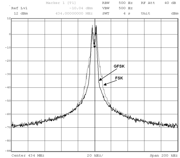
The data modulator can modulate FSK, which is a two level FSK (Frequency Shift Keying), or GFSK, which is a Gaussian filtered FSK with BT = 0.5. The purpose of the GFSK is to make a more bandwidth efficient system as shown in Figure 5-17. The modulation and the Gaussian filtering are done internally in the chip. The TX_SHAPING bit in the DEVIATION register enables the GFSK. GFSK is recommended for narrowband operation.
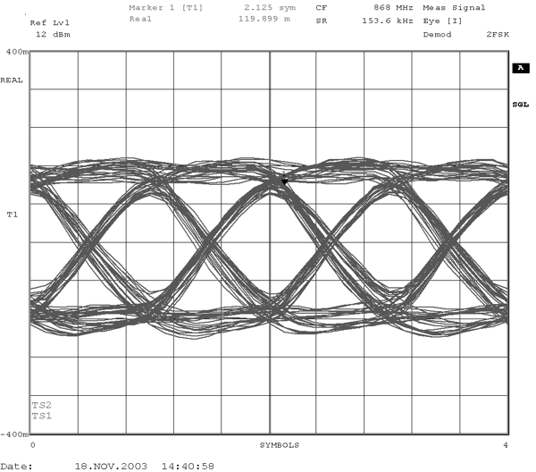
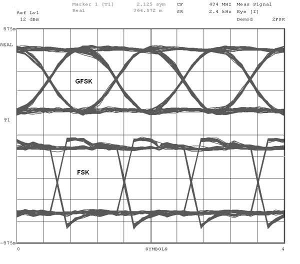
Figure 5-18 and Figure 5-19 show typical eye diagrams for 434 MHz and 868 MHz operation, respectively.

| 2.4 kBaud, | NRZ, | ±2.025 kHz frequency deviation |

| 153.6 kBaud, | NRZ, | ±79.2 kHz frequency deviation | ||

| 2.4 kBaud, | NRZ, | ±2.025 kHz frequency deviation |