SWRS178C February 2015 – July 2016 CC2620
PRODUCTION DATA.
- 1Device Overview
- 2Revision History
- 3 Device Comparison
- 4Terminal Configuration and Functions
-
5Specifications
- 5.1 Absolute Maximum Ratings
- 5.2 ESD Ratings
- 5.3 Recommended Operating Conditions
- 5.4 Power Consumption Summary
- 5.5 General Characteristics
- 5.6 IEEE 802.15.4 (Offset Q-PSK DSSS, 250 kbps) - RX
- 5.7 IEEE 802.15.4 (Offset Q-PSK DSSS, 250 kbps) - TX
- 5.8 24-MHz Crystal Oscillator (XOSC_HF)
- 5.9 32.768-kHz Crystal Oscillator (XOSC_LF)
- 5.10 48-MHz RC Oscillator (RCOSC_HF)
- 5.11 32-kHz RC Oscillator (RCOSC_LF)
- 5.12 ADC Characteristics
- 5.13 Temperature Sensor
- 5.14 Battery Monitor
- 5.15 Continuous Time Comparator
- 5.16 Low-Power Clocked Comparator
- 5.17 Programmable Current Source
- 5.18 Synchronous Serial Interface (SSI)
- 5.19 DC Characteristics
- 5.20 Thermal Resistance Characteristics
- 5.21 Timing Requirements
- 5.22 Switching Characteristics
- 5.23 Typical Characteristics
- 6Detailed Description
- 7Application, Implementation, and Layout
- 8Device and Documentation Support
- 9Mechanical Packaging and Orderable Information
Package Options
Mechanical Data (Package|Pins)
Thermal pad, mechanical data (Package|Pins)
Orderable Information
7 Application, Implementation, and Layout
NOTE
Information in the following applications sections is not part of the TI component specification, and TI does not warrant its accuracy or completeness. TI's customers are responsible for determining suitability of components for their purposes. Customers should validate and test their design implementation to confirm system functionality.
7.1 Application Information
Very few external components are required for the operation of the CC2620 device. This section provides some general information about the various configuration options when using the CC2620 in an application, and then shows two examples of application circuits with schematics and layout. This is only a small selection of the many application circuit examples available as complete reference designs from the product folder on www.ti.com.
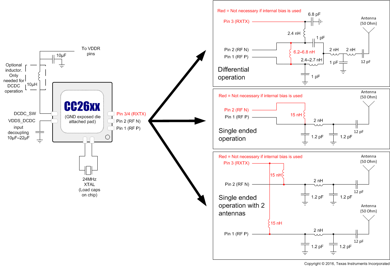
Figure 7-1 shows the various RF front-end configuration options. The RF front end can be used in differential- or single-ended configurations with the options of having internal or external biasing. These options allow for various trade-offs between cost, board space, and RF performance. Differential operation with external bias gives the best performance while single-ended operation with internal bias gives the least amount of external components and the lowest power consumption. Reference designs exist for each of these options.
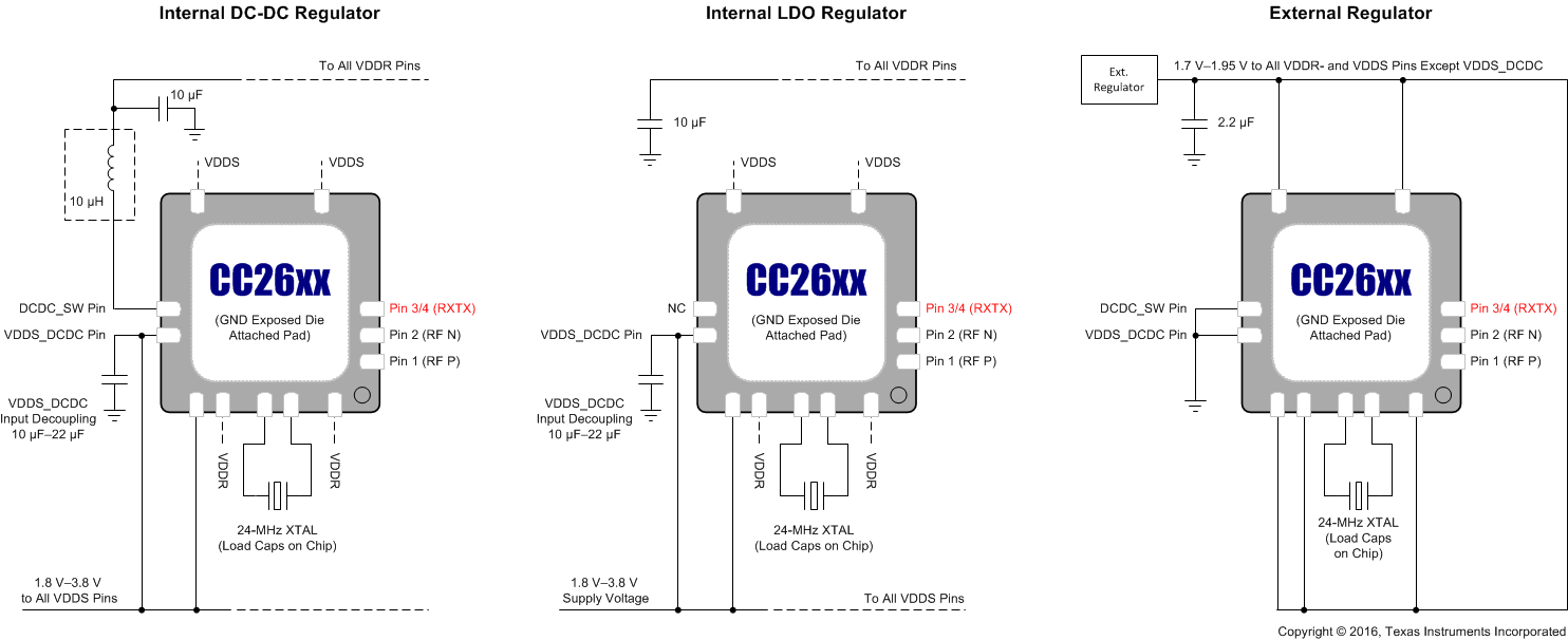
Figure 7-2 shows the various supply voltage configuration options. Not all power supply decoupling capacitors or digital I/Os are shown. Exact pin positions will vary between the different package options. For a detailed overview of power supply decoupling and wiring, see the TI reference designs and the CC26xx technical reference manual (Section 8.3).
 Figure 7-2 Supply Voltage Configurations
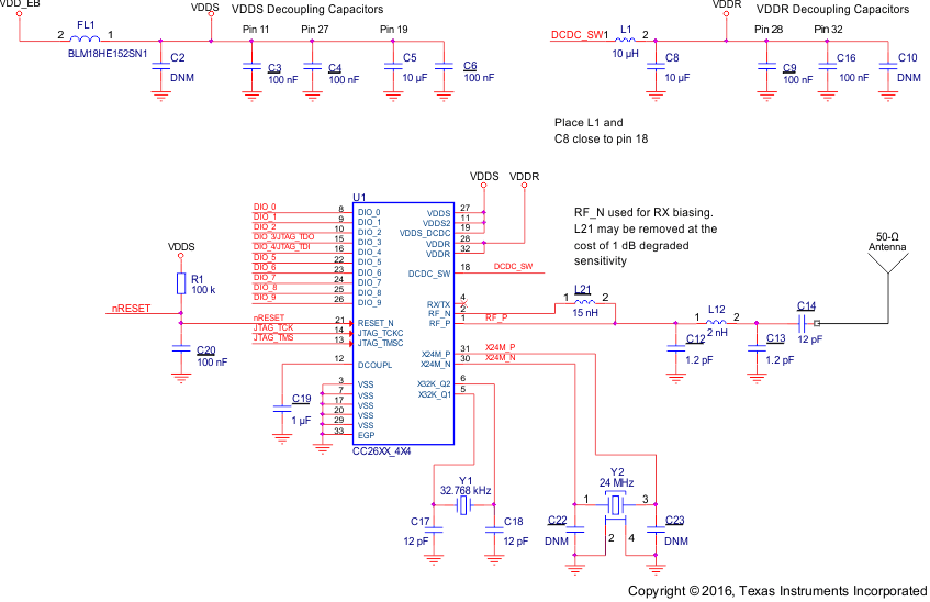
7.2 4 × 4 External Single-ended (4XS) Application Circuit
 Figure 7-3 4 × 4 External Single-ended (4XS) Application Circuit
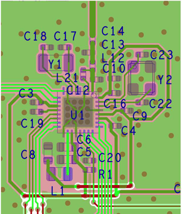
7.2.1 Layout
 Figure 7-4 4 × 4 External Single-ended (4XS) Layout
