SWAS031D June 2013 – February 2015 CC3100
PRODUCTION DATA.
- 1Device Overview
- 2Revision History
- 3Terminal Configuration and Functions
-
4Specifications
- 4.1 Absolute Maximum Ratings
- 4.2 Handling Ratings
- 4.3 Power-On Hours
- 4.4 Recommended Operating Conditions
- 4.5 Brown-Out and Black-Out
- 4.6 Electrical Characteristics (3.3 V, 25°C)
- 4.7 WLAN Receiver Characteristics
- 4.8 WLAN Transmitter Characteristics
- 4.9 Current Consumption
- 4.10 Thermal Characteristics for RGC Package
- 4.11 Timing and Switching Characteristics
- 4.12 External Interfaces
- 4.13 Host UART
- 5Detailed Description
- 6Applications and Implementation
- 7Device and Documentation Support
- 8Mechanical Packaging and Orderable Information
Package Options
Mechanical Data (Package|Pins)
- RGC|64
Thermal pad, mechanical data (Package|Pins)
- RGC|64
Orderable Information
5 Detailed Description
5.1 Overview
5.1.1 Device Features
5.1.1.1 WLAN
- 802.11b/g/n integrated radio, modem, and MAC supporting WLAN communication as a BSS station with CCK and OFDM rates in the 2.4-GHz ISM band
- Auto-calibrated radio with a single-ended 50-Ω interface enables easy connection to the antenna without requiring expertise in radio circuit design.
- Advanced connection manager with multiple user-configurable profiles stored in an NVMEM allows automatic fast connection to an access point without user or host intervention.
- Supports all common Wi-Fi security modes for personal and enterprise networks with on-chip security accelerators
- SmartConfig technology: A 1-step, 1-time process to connect a CC3100-enabled device to the home wireless network, removing dependency on the I/O capabilities of the host MCU; thus, it is usable by deeply embedded applications.
- 802.11 transceiver mode: Allows transmitting and receiving of proprietary data through a socket without adding MAC or PHY headers. This mode provides the option to select the working channel, rate, and transmitted power. The receiver mode works together with the filtering options.
5.1.1.2 Network Stack
- Integrated IPv4 TCP/IP stack with BSD socket APIs for simple Internet connectivity with any MCU, microprocessor, or ASIC
- Support of eight simultaneous TCP, UDP, or RAW sockets
- Built-in network protocols: ARP, ICMP, DHCP client, and DNS client for easy connection to the local network and the Internet
- Service discovery: Multicast DNS service discovery lets a client advertise its service without a centralized server. After connecting to the access point, the CC3100 device provides critical information, such as device name, IP, vendor, and port number.
5.1.1.3 Host Interface and Driver
- Interfaces over a 4-wire serial peripheral interface (SPI) with any MCU or a processor at a clock speed of 20 MHz.
- Interfaces over UART with any MCU with a baud rate up to 3 Mbps. A low footprint driver is provided for TI MCUs and is easily ported to any processor or ASIC.
- Simple APIs enable easy integration with any single-threaded or multithreaded application.
5.1.1.4 System
- Works from a single preregulated power supply or connects directly to a battery
- Ultra-low leakage when disabled (hibernate mode) with a current of less than 4 µA with the RTC running
- Integrated clock sources
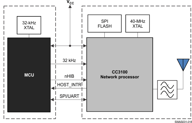
5.2 Functional Block Diagram
Figure 5-1 shows the functional block diagram of the CC3100 SimpleLink Wi-Fi solution.
5.3 Wi-Fi Network Processor Subsystem
The Wi-Fi network processor subsystem includes a dedicated ARM MCU to completely offload the host MCU along with an 802.11 b/g/n radio, baseband, and MAC with a powerful crypto engine for a fast, secure WLAN and Internet connections with 256-bit encryption. The CC3100 device supports station, AP, and Wi-Fi Direct modes. The device also supports WPA2 personal and enterprise security and WPS 2.0. The Wi-Fi network processor includes an embedded IPv4 TCP/IP stack.
Table 5-1 summarizes the NWP features.
Table 5-1 Summary of Features Supported by the NWP Subsystem
| Item | Domain | Category | Feature | Details |
|---|---|---|---|---|
| 1 | TCP/IP | Network Stack | IPv4 | Baseline IPv4 stack |
| 2 | TCP/IP | Network Stack | TCP/UDP | Base protocols |
| 3 | TCP/IP | Protocols | DHCP | Client and server mode |
| 4 | TCP/IP | Protocols | ARP | Support ARP protocol |
| 5 | TCP/IP | Protocols | DNS/mDNS | DNS Address resolution and local server |
| 6 | TCP/IP | Protocols | IGMP | Up to IGMPv3 for multicast management |
| 7 | TCP/IP | Applications | mDNS | Support multicast DNS for service publishing over IP |
| 8 | TCP/IP | Applications | mDNS-SD | Service discovery protocol over IP in local network |
| 9 | TCP/IP | Applications | Web Sever/HTTP Server | URL static and dynamic response with template. |
| 10 | TCP/IP | Security | TLS/SSL | TLS v1.2 (client/server)/SSL v3.0 |
| 11 | TCP/IP | Security | TLS/SSL | For the supported Cipher Suite, go to SimpleLink Wi-Fi CC3100 SDK. |
| 12 | TCP/IP | Sockets | RAW Sockets | User-defined encapsulation at WLAN MAC/PHY or IP layers |
| 13 | WLAN | Connection | Policies | Allows management of connection and reconnection policy |
| 14 | WLAN | MAC | Promiscuous mode | Filter-based Promiscuous mode frame receiver |
| 15 | WLAN | Performance | Initialization time | From enable to first connection to open AP less than 50 ms |
| 16 | WLAN | Performance | Throughput | UDP = 16 Mbps |
| 17 | WLAN | Performance | Throughput | TCP = 13 Mbps |
| 18 | WLAN | Provisioning | WPS2 | Enrollee using push button or PIN method. |
| 19 | WLAN | Provisioning | AP Config | AP mode for initial product configuration (with configurable Web page and beacon Info element) |
| 20 | WLAN | Provisioning | SmartConfig | Alternate method for initial product configuration |
| 21 | WLAN | Role | Station | 802.11bgn Station with legacy 802.11 power save |
| 22 | WLAN | Role | Soft AP | 802.11 bg single station with legacy 802.11 power save |
| 23 | WLAN | Role | P2P | P2P operation as GO |
| 24 | WLAN | Role | P2P | P2P operation as CLIENT |
| 25 | WLAN | Security | STA-Personal | WPA2 personal security |
| 26 | WLAN | Security | STA-Enterprise | WPA2 enterprise security |
| 27 | WLAN | Security | STA-Enterprise | EAP-TLS |
| 28 | WLAN | Security | STA-Enterprise | EAP-PEAPv0/TLS |
| 29 | WLAN | Security | STA-Enterprise | EAP-PEAPv1/TLS |
| 30 | WLAN | Security | STA-Enterprise | EAP-PEAPv0/MSCHAPv2 |
| 31 | WLAN | Security | STA-Enterprise | EAP-PEAPv1/MSCHAPv2 |
| 32 | WLAN | Security | STA-Enterprise | EAP-TTLS/EAP-TLS |
| 33 | WLAN | Security | STA-Enterprise | EAP-TTLS/MSCHAPv2 |
| 34 | WLAN | Security | AP-Personal | WPA2 personal security |
5.4 Power-Management Subsystem
The CC3100 power-management subsystem contains DC-DC converters to accommodate the differing voltage or current requirements of the system.
- Digital DC-DC
- Input: VBAT wide voltage (2.1 to 3.6 V) or preregulated 1.85 V
- ANA1 DC-DC
- Input: VBAT wide voltage (2.1 to 3.6 V)
- In preregulated 1.85-V mode, the ANA1 DC-DC converter is bypassed.
- PA DC-DC
- Input: VBAT wide voltage (2.1 to 3.6 V)
- In preregulated 1.85-V mode, the PA DC-DC converter is bypassed.
In preregulated 1.85-V mode, the ANA1 DC-DC and PA DC-DC converters are bypassed. The CC3100 device is a single-chip WLAN radio solution used on an embedded system with a wide-voltage supply range. The internal power management, including DC-DC converters and LDOs, generates all of the voltages required for the device to operate from a wide variety of input sources. For maximum flexibility, the device can operate in the modes described in the following sections.
5.4.1 VBAT Wide-Voltage Connection
In the wide-voltage battery connection, the device is powered directly by the battery. All other voltages required to operate the device are generated internally by the DC-DC converters. This scheme is the most common mode for the device as it supports wide-voltage operation from 2.1 to 3.6 V (for electrical connections, see Section 6.1.1, Typical Application – CC3100 Wide-Voltage Mode).
5.4.2 Preregulated 1.85 V
The preregulated 1.85-V mode of operation applies an external regulated 1.85 V directly at the pins 10, 25, 33, 36, 37, 39, 44, 48, and 54 of the device. The VBAT and the VIO are also connected to the 1.85-V supply. This mode provides the lowest BOM count version in which inductors used for PA DC-DC and ANA1 DC-DC (2.2 and 1 µH) and a capacitor (22 µF) can be avoided. For electrical connections, see Section 6.1.2, Typical Application – CC3100 Preregulated 1.85-V Mode.
In the preregulated 1.85-V mode, the regulator providing the 1.85 V must have the following characteristics:
- Load current capacity ≥900 mA.
- Line and load regulation with <2% ripple with 500 mA step current and settling time of <4 µs with the load step.
- The regulator must be placed very close to the CC3100 device so that the IR drop to the device is very low.
5.5 Low-Power Operating Modes
This section describes the low-power modes supported by the device to optimize battery life.
5.5.1 Low-Power Deep Sleep
The low-power deep-sleep (LPDS) mode is an energy-efficient and transparent sleep mode that is entered automatically during periods of inactivity based on internal power optimization algorithms. The device can wake up in less than 3 ms from the internal timer or from any incoming host command. Typical battery drain in this mode is 115 µA. During LPDS mode, the device retains the software state and certain configuration information. The operation is transparent to the external host; thus, no additional handshake is required to enter or exit this sleep mode.
5.5.2 Hibernate
The hibernate mode is the lowest power mode in which all of the digital logic is power-gated. Only a small section of the logic powered directly by the main input supply is retained. The real-time clock (RTC) is kept running and the device wakes up once the nHIB line is asserted by the host driver. The wake-up time is longer than LPDS mode at about 50 ms.
NOTE
Wake-up time can be extended to 75 ms if a patch is loaded from the serial flash.
5.6 Memory
5.6.1 External Memory Requirements
The CC3100 device maintains a proprietary file system on the SFLASH. The CC3100 file system stores the service pack file, system files, configuration files, certificate files, web page files, and user files. By using a format command through the API, users can provide the total size allocated for the file system. The starting address of the file system cannot be set and is always located at the beginning of the SFLASH. The applications microcontroller must access the SFLASH memory area allocated to the file system directly through the CC3100 file system. The applications microcontroller must not access the SFLASH memory area directly.
The file system manages the allocation of SFLASH blocks for stored files according to download order, which means that the location of a specific file is not fixed in all systems. Files are stored on SFLASH using human-readable file names rather than file IDs. The file system API works using plain text, and file encryption and decryption is invisible to the user. Encrypted files can be accessed only through the file system.
All file types can have a maximum of 128 supported files in the file system. All files are stored in blocks of 4KB and thus use a minimum of 4KB of flash space. Encrypted files with fail-safe support and optional security are twice the original size and use a minimum of 8KB. Encrypted files are counted as fail safe in terms of space. The maximum file size is 16MB.
Table 5-2 lists the SFLASH size recommendations.
Table 5-2 CC3100 SFLASH Size Recommendations
| Item | Typical Fail-Safe | Typical NonFail-Safe |
|---|---|---|
| File system | 20KB | 20KB |
| Service pack | 224KB | 112KB |
| System and configuration files | 216KB | 108KB |
| Total | 4Mb | 2Mb |
| Recommended | 8Mb | 4Mb |
The CC3100 device supports JEDEC specification SFDP (serial flash device parameters). The following SFLASH devices are verified for functionality with the CC3100 device in addition to the ones in the reference design:
- Micron (N25Q128-A13BSE40): 128Mb
- Spansion (S25FL208K): 8Mb
- Winbond (W25Q16V): 16Mb
- Adesto (AT25DF081A): 8Mb
- Macronix (MX25L12835F-M2): 128Mb
For compatibility with the CC3100 device, the SFLASH device must support the following commands:
- Command 0x9F (read the device ID [JEDEC]). Procedure: SEND 0x9F, READ 3 bytes.
- Command 0x05 (read the status of the SFLASH). Procedure: SEND 0x05, READ 1 byte. Assume bit 0 is busy and bit 1 is write enable.
- Command 0x06 (set write enable). Procedure: SEND 0x06, read status until write-enable bit is set.
- Command 0xC7 (chip erase). Procedure: SEND 0xC7, read status until busy bit is cleared.
- Command 0x03 (read data). Procedure: SEND 0x03, SEND 24-bit address, read n bytes.
- Command 0x02 (write page). Procedure: SEND 0x02, SEND 24-bit address, write n bytes (0<n<256).
- Command 0x20 (sector erase). Procedure: SEND 0x20, SEND 24-bit address, read status until busy bit is cleared. Sector size is assumed to be always 4K.