SLAS555B June 2012 – September 2018 CC430F5123 , CC430F5125 , CC430F5143 , CC430F5145 , CC430F5147 , CC430F6147
PRODUCTION DATA.
- 1Device Overview
- 2Revision History
- 3Device Comparison
- 4Terminal Configuration and Functions
-
5Specifications
- 5.1 Absolute Maximum Ratings
- 5.2 ESD Ratings
- 5.3 Recommended Operating Conditions
- 5.4 Active Mode Supply Current Into VCC Excluding External Current
- 5.5 Typical Characteristics – Active Mode Supply Currents
- 5.6 Low-Power Mode Supply Currents (Into VCC) Excluding External Current
- 5.7 Typical Characteristics – Low-Power Mode Supply Currents
- 5.8 Low-Power Mode With LCD Supply Currents (Into VCC) Excluding External Current
- 5.9 Thermal Resistance Characteristics, CC430F51xx
- 5.10 Thermal Resistance Characteristics, CC430F61xx
- 5.11 Digital Inputs
- 5.12 Digital Outputs
- 5.13 Typical Characteristics – Outputs, Reduced Drive Strength (PxDS.y = 0)
- 5.14 Typical Characteristics – Outputs, Full Drive Strength (PxDS.y = 1)
- 5.15 Crystal Oscillator, XT1, Low-Frequency Mode
- 5.16 Internal Very-Low-Power Low-Frequency Oscillator (VLO)
- 5.17 Internal Reference, Low-Frequency Oscillator (REFO)
- 5.18 DCO Frequency
- 5.19 PMM, Brownout Reset (BOR)
- 5.20 PMM, Core Voltage
- 5.21 PMM, SVS High Side
- 5.22 PMM, SVM High Side
- 5.23 PMM, SVS Low Side
- 5.24 PMM, SVM Low Side
- 5.25 Wake-up Times From Low-Power Modes and Reset
- 5.26 Timer_A
- 5.27 USCI (UART Mode) Clock Frequency
- 5.28 USCI (UART Mode)
- 5.29 USCI (SPI Master Mode) Clock Frequency
- 5.30 USCI (SPI Master Mode)
- 5.31 USCI (SPI Slave Mode)
- 5.32 USCI (I2C Mode)
- 5.33 LCD_B Operating Conditions
- 5.34 LCD_B Electrical Characteristics
- 5.35 10-Bit ADC, Power Supply and Input Range Conditions
- 5.36 10-Bit ADC, Timing Parameters
- 5.37 10-Bit ADC, Linearity Parameters
- 5.38 REF, External Reference
- 5.39 REF, Built-In Reference
- 5.40 Comparator_B
- 5.41 Flash Memory
- 5.42 JTAG and Spy-Bi-Wire Interface
- 5.43
RF1A CC1101-Based Radio Parameters
- 5.43.1 RF1A Recommended Operating Conditions
- 5.43.2 RF Crystal Oscillator, XT2
- 5.43.3 Current Consumption, Reduced-Power Modes
- 5.43.4 Current Consumption, Receive Mode
- 5.43.5 Current Consumption, Transmit Mode
- 5.43.6 Typical TX Current Consumption, 315 MHz, 25°C
- 5.43.7 Typical TX Current Consumption, 433 MHz, 25°C
- 5.43.8 Typical TX Current Consumption, 868 MHz
- 5.43.9 Typical TX Current Consumption, 915 MHz
- 5.43.10 RF Receive, Overall
- 5.43.11 RF Receive, 315 MHz
- 5.43.12 RF Receive, 433 MHz
- 5.43.13 RF Receive, 868 MHz and 915 MHz
- 5.43.14 Typical Sensitivity, 315 MHz, Sensitivity Optimized Setting
- 5.43.15 Typical Sensitivity, 433 MHz, Sensitivity Optimized Setting
- 5.43.16 Typical Sensitivity, 868 MHz, Sensitivity Optimized Setting
- 5.43.17 Typical Sensitivity, 915 MHz, Sensitivity Optimized Setting
- 5.43.18 RF Transmit
- 5.43.19 Optimum PATABLE Settings for Various Output Power Levels and Frequency Bands
- 5.43.20 Typical Output Power, 315 MHz
- 5.43.21 Typical Output Power, 433 MHz
- 5.43.22 Typical Output Power, 868 MHz
- 5.43.23 Typical Output Power, 915 MHz
- 5.43.24 Frequency Synthesizer Characteristics
- 5.43.25 Typical RSSI_offset Values
-
6Detailed Description
- 6.1 Sub-1 GHz Radio
- 6.2 CPU
- 6.3 Operating Modes
- 6.4 Interrupt Vector Addresses
- 6.5 Memory Organization
- 6.6 Bootloader (BSL)
- 6.7 JTAG Operation
- 6.8 Flash Memory
- 6.9 RAM
- 6.10 Backup RAM
- 6.11
Peripherals
- 6.11.1 Oscillator and System Clock
- 6.11.2 Power-Management Module (PMM)
- 6.11.3 Digital I/O
- 6.11.4 Port Mapping Controller
- 6.11.5 System Module (SYS)
- 6.11.6 DMA Controller
- 6.11.7 Watchdog Timer (WDT_A)
- 6.11.8 CRC16
- 6.11.9 Hardware Multiplier
- 6.11.10 AES128 Accelerator
- 6.11.11 Universal Serial Communication Interface (USCI)
- 6.11.12 TA0
- 6.11.13 TA1
- 6.11.14 Real-Time Clock (RTC_D)
- 6.11.15 Voltage Reference (REF) (Including Output)
- 6.11.16 LCD_B (Only CC430F614x)
- 6.11.17 Comparator_B
- 6.11.18 ADC10_A (CC430F614x and CC430F514x Only)
- 6.11.19 Embedded Emulation Module (EEM) (S Version)
- 6.11.20 Peripheral File Map
- 6.12
Input/Output Diagrams
- 6.12.1 Port P1 (P1.0 to P1.4) Input/Output With Schmitt Trigger
- 6.12.2 Port P1 (P1.5 to P1.7) Input/Output With Schmitt Trigger
- 6.12.3 Port P2 (P2.0 to P2.7) Input/Output With Schmitt Trigger
- 6.12.4 Port P3 (P3.0 to P3.7) Input/Output With Schmitt Trigger
- 6.12.5 Port P4 (P4.0 to P4.7) Input/Output With Schmitt Trigger (CC430F614x Only)
- 6.12.6 Port P5 (P5.0 and P5.1) Input/Output With Schmitt Trigger
- 6.12.7 Port P5 (P5.2 to P5.4) Input/Output With Schmitt Trigger (CC430F614x Only)
- 6.12.8 Port P5 (P5.5 to P5.7) Input/Output With Schmitt Trigger (CC430F614x Only)
- 6.12.9 Port PJ (PJ.0) JTAG Pin TDO, Input/Output With Schmitt Trigger or Output
- 6.12.10 Port PJ (PJ.1 to PJ.3) JTAG Pins TMS, TCK, TDI/TCLK, Input/Output With Schmitt Trigger or Output
- 6.13 Device Descriptor Structure
- 7Applications, Implementation, and Layout
- 8Device and Documentation Support
- 9Mechanical, Packaging, and Orderable Information
Package Options
Mechanical Data (Package|Pins)
- RGZ|48
Thermal pad, mechanical data (Package|Pins)
- RGZ|48
Orderable Information
7.1 Application Circuits
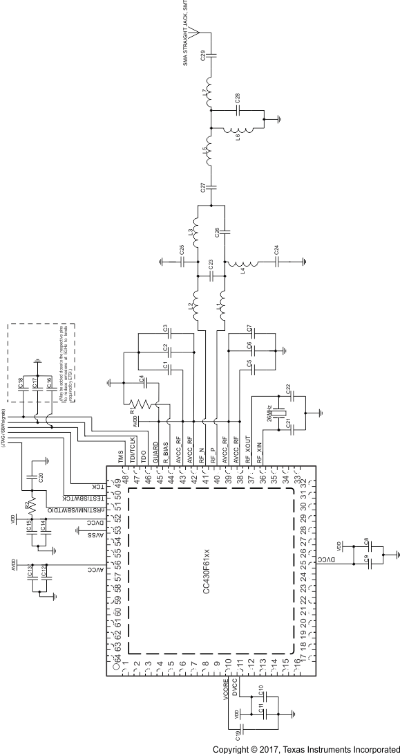
Figure 7-1 shows a typical application circuit for the CC430F61xx. Table 7-1 lists the bill of materials.

For a complete reference design including layout, see the CC430 wireless development tools, their related documentation, and the MSP430 Hardware Tools User's Guide.
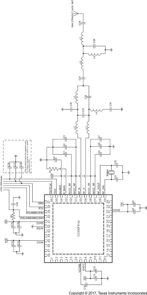
Figure 7-1 Typical Application Circuit CC430F61xx Figure 7-2 shows a typical application circuit for the CC430F51xx. Table 7-1 lists the bill of materials.

For a complete reference design including layout, see the CC430 wireless development tools, their related documentation, and the MSP430 Hardware Tools User's Guide.
Figure 7-2 Typical Application Circuit CC430F51xx Table 7-1 Bill of Materials
| COMPONENTS | FOR 315 MHz | FOR 433 MHz | FOR 868 or 915 MHz | COMMENT |
|---|---|---|---|---|
| C1, C3, C4, C5, C7, C9, C11, C13, C15 | 100 nF | Decoupling capacitors | ||
| C8, C10, C12, C14 | 10 µF | Decoupling capacitors | ||
| C2, C6, C16, C17, C18 | 2 pF | Decoupling capacitors | ||
| C19 | 470 nF | VCORE capacitor | ||
| C20 | 2.2 nF | RST decoupling cap (optimized for SBW) | ||
| C21, C22 | 27 pF | Load capacitors for 26-MHz crystal(1) | ||
| R1 | 56 kΩ | R_BIAS (±1% required) | ||
| R2 | 47kΩ | RST pullup | ||
| L1, L2 | Capacitors: 220 pF | 0.016 µH | 0.012 µH | |
| L3, L4 | 0.033 µH | 0.027 µH | 0.018 µH | |
| L5 | 0.033 µH | 0.047 µH | 0.015 µH | |
| L6 | dnp(2) | dnp(2) | 0.0022 µH | |
| L7 | 0.033 µH | 0.051 µH | 0.015 µH | |
| C23 | dnp(2) | 2.7 pF | 1 pF | |
| C24 | 220 pF | 220 pF | 100 pF | |
| C25 | 6.8 pF | 3.9 pF | 1.5 pF | |
| C26 | 6.8 pF | 3.9 pF | 1.5 pF | |
| C27 | 220 pF | 220 pF | 1.5 pF | |
| C28 | 10 pF | 4.7 pF | 8.2 pF | |
| C29 | 220 pF | 220 pF | 1.5 pF | |
(1) The load capacitance CL seen by the crystal is CL = 1 / ((1 / C21) + (1 / C22)) + Cparasitic. The parasitic capacitance Cparasitic includes pin capacitance and PCB stray capacitance. It can be typically estimated to be approximately 2.5 pF.
(2) dnp = do not populate