SCHS168E November 1998 – March 2022 CD54HC243 , CD74HC243 , CD74HCT243
PRODUCTION DATA
- 1 Features
- 2 Description
- 3 Revision History
- 4 Pin Configuration and Functions
- 5 Specifications
- 6 Parameter Measurement Information
- 7 Detailed Description
- 8 Power Supply Recommendations
- 9 Layout
- 10Device and Documentation Support
- 11Mechanical, Packaging, and Orderable Information
Package Options
Refer to the PDF data sheet for device specific package drawings
Mechanical Data (Package|Pins)
- J|14
Thermal pad, mechanical data (Package|Pins)
Orderable Information
2 Description
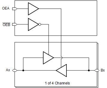
The CDx4HC243 and CDx4HCT243 are quad bus transceivers with 3-state outputs. The OEA and OEB inputs control both the high-impedance state as well as the direction of communication through the device.
Device Information
| PART NUMBER | PACKAGE(1) | BODY SIZE (NOM) |
|---|---|---|
| CD54HC243F | CDIP (14) | 19.55 mm × 6.71 mm |
| CD74HC243E | PDIP (14) | 19.31 mm × 6.35 mm |
| CD74HC243M | SOIC (14) | 8.65 mm × 3.90 mm |
| CD74HCT243E | PDIP (14) | 19.31 mm × 6.35 mm |
| CD74HCT243M | SOIC (14) | 8.65 mm × 3.90 mm |
(1) For all packages see the
orderable addendum at the end of the datasheet.
 Functional Block
Diagram