SCHS147J November 1998 – November 2021 CD54HC138 , CD54HC238 , CD54HCT138 , CD54HCT238 , CD74HC138 , CD74HC238 , CD74HCT138 , CD74HCT238
PRODUCTION DATA
- 1 Features
- 2 Description
- 3 Revision History
- 4 Pin Configuration and Functions
- 5 Specifications
- 6 Parameter Measurement Information
- 7 Detailed Description
- 8 Power Supply Recommendations
- 9 Layout
- 10Device and Documentation Support
- 11Mechanical, Packaging, and Orderable Information
Package Options
Refer to the PDF data sheet for device specific package drawings
Mechanical Data (Package|Pins)
- PW|16
- N|16
- D|16
Thermal pad, mechanical data (Package|Pins)
Orderable Information
1 Features
- Select one of eight data outputs:
- Active low for '138
- Active high for '238
- l/O port or memory selector
- Three enable inputs to simplify cascading
- Typical propagation delay of 13 ns at VCC = 5 V, CL = 15 pF, TA = 25°C
- Fanout (over temperature range)
- Bus driver outputs: 15 LSTTL loads
- Standard outputs: 10 LSTTL loads
- Wide operating temp range: -55°C to 125°C
- Balanced propagation delay and transition times
- Significant power reduction compared to LSTTL logic ICs
- HC types
- 2 V to 6 V operation
- High noise immunity: NIL = 30%, NIH = 30% of VCC at VCC = 5 V
- HCT types
- 4.5-V to 5.5-V operation
- Direct LSTTL input logic compatibility, VIL= 0.8 V (Max), VIH = 2 V (Min)
- CMOS input compatibility, Il ≤ 1µA at VOL, VOH
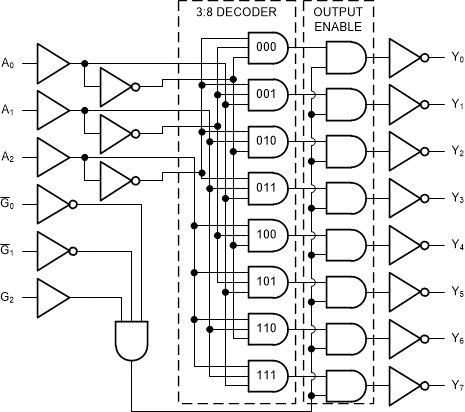
 Functional Block Diagram
'138