SLLSEL1 November 2014 CDCL1810A
PRODUCTION DATA.
- 1 Features
- 2 Applications
- 3 Description
- 4 Simplified Schematic
- 5 Revision History
- 6 Device Comparison Tables
- 7 Pin Configuration and Functions
- 8 Specifications
- 9 Detailed Description
- 10Application and Implementation
- 11Power Supply Recommendations
- 12Layout
- 13Device and Documentation Support
- 14Mechanical, Packaging, and Orderable Information
- 13Mechanical, Packaging, and Orderable Information
Package Options
Mechanical Data (Package|Pins)
- RGZ|48
Thermal pad, mechanical data (Package|Pins)
- RGZ|48
Orderable Information
1 Features
- Single 1.8 V Supply
- High-Performance Clock Distributor with 10 Outputs
- Low Input-to-Output Additive Jitter: as low as 10fs RMS
- Low-Voltage Differential Signaling (LVDS) Input, 100Ω Differential On-Chip Termination, up to 650 MHz Frequency
- Differential Current Mode Logic (CML) Outputs, 50Ω Single-Ended On-Chip Termination, up to 650 MHz Frequency
- Two Groups of Five Outputs Each with Independent Frequency Division Ratios
- Output Frequency Derived with Divide Ratios of 1, 2, 4, 5, 8, 10, 16, 20, 32, 40, and 80
- Meets ANSI TIA/EIA-644-A-2001 LVDS Standard Requirements
- Power Consumption: 410 mW Typical
- Output Enable Control for Each Output
- SDA/SCL Device Management Interface
- 48-pin VQFN (RGZ) Package
- Industrial Temperature Range: –40°C to +85°C
2 Applications
- Clock Distribution for High-Speed SERDES
- Distribution of SERDES Reference Clocks for 1G/10G Ethernet, 1X/2X/4X/10X Fibre Channel, PCI Express, Serial ATA, SONET, CPRI, OBSAI, and so forth
- Up to 1-to-10 Clock Buffering and Fan-out
3 Description
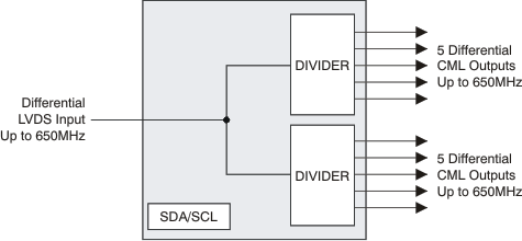
The CDCL1810A is a high-performance clock distributor. The programmable dividers, P0 and P1, give a high flexibility to the ratio of the output frequency to the input frequency: FOUT = FIN/P, where P (P0,P1) = 1, 2, 4, 5, 8, 10, 16, 20, 32, 40, 80.
The CDCL1810A supports one differential LVDS clock input and a total of 10 differential CML outputs. The CML outputs are compatible with LVDS receivers if they are ac-coupled.
With careful observation of the input voltage swing and common-mode voltage limits, the CDCL1810A can support a single-ended clock input as outlined in Pin Configuration and Functions.
All device settings are programmable through the SDA/SCL, serial two-wire interface. The serial interface is 1.8V tolerant only.
The device operates in a 1.8V supply environment and is characterized for operation from –40°C to +85°C. The CDCL1810A is available in a 48-pin QFN (RGZ) package.
Device Information(1)
| PART NUMBER | PACKAGE | BODY SIZE (NOM) |
|---|---|---|
| CDCL1810A | VQFN (48) | 7.00 mm × 7.00 mm |
- For all available packages, see the orderable addendum at the end of the datasheet.
4 Simplified Schematic