SCAS951 April 2017 CDCS504-Q1
PRODUCTION DATA.
- 1 Features
- 2 Applications
- 3 Description
- 4 Revision History
- 5 Pin Configuration and Functions
- 6 Specifications
- 7 Parameter Measurement Information
- 8 Detailed Description
- 9 Application and Implementation
- 10Power Supply Recommendations
- 11Layout
- 12Device And Documentation Support
- 13Mechanical, Packaging, and Orderable Information
Package Options
Mechanical Data (Package|Pins)
- PW|8
Thermal pad, mechanical data (Package|Pins)
Orderable Information
1 Features
- Qualified for Automotive Applications
- AEC-Q100 Test Guidance With the Following Results:
- Device Temperature Grade 2: –40°C to 105°C Ambient Operating Temperature Range
- Device HBM ESD Classification Level H2
- Device CDM ESD Classification Level C3B
- Part of a Family of Easy-to-Use Clock Generator Devices
- Clock Multiplier With Selectable Output Frequency
- Frequency Multiplication Selectable Between x1 or x4 With One External Control Pin
- Output Disable Through Control Pin
- Single 3.3-V Device Power Supply
- Wide Temperature Range: –40°C to 105°C
- Low Space Consumption 8-Pin TSSOP Package
- Create a Custom Design Using the CDCS504-Q1 With the WEBENCH® Power Designer
2 Applications
Automotive Applications Requiring Clock
Multiplication
3 Description
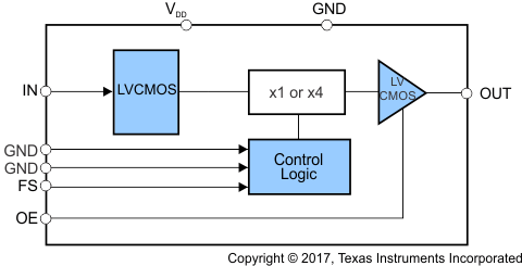
The CDCS504-Q1 device is a LVCMOS input clock buffer with selectable frequency multiplication.
The CDCS504-Q1 has an output enable pin.
The device accepts a 3.3-V LVCMOS signal at the input.
The input signal is processed by a phased-locked loop (PLL), whose output frequency is either equal to the input frequency or multiplied by the factor of four.
By this, the device can generate output frequencies between 2 MHz and 108 MHz.
A separate control pin can be used to enable or disable the output. The CDCS504-Q1 device operates in a 3.3-V environment.
It is characterized for operation from –40°C to 105°C and is available in an 8-pin TSSOP package.
Device Information(1)
| PART NUMBER | PACKAGE | BODY SIZE (NOM) |
|---|---|---|
| CDCS504-Q1 | TSSOP (8) | 3.00 mm × 4.40 mm |
- For all available packages, see the orderable addendum at the end of the data sheet.
Block Diagram
