SLPS306A May 2012 – September 2015 CSD13201W10
PRODUCTION DATA.
- 1Features
- 2Applications
- 3Description
- 4Revision History
- 5Specifications
- 6Device and Documentation Support
- 7Mechanical, Packaging, and Orderable Information
Package Options
Mechanical Data (Package|Pins)
- YZB|4
Thermal pad, mechanical data (Package|Pins)
Orderable Information
5 Specifications
5.1 Electrical Characteristics
TA = 25°C (unless otherwise noted)| PARAMETER | TEST CONDITIONS | MIN | TYP | MAX | UNIT | |
|---|---|---|---|---|---|---|
| STATIC CHARACTERISTICS | ||||||
| BVDSS | Drain-to-source voltage | VGS = 0 V, ID = 250 μA | 12 | V | ||
| IDSS | Drain-to-source leakage current | VGS = 0 V, VDS = 9.6 V | 1 | μA | ||
| IGSS | Gate-to-source leakage current | VDS = 0 V, VGS = 8 V | 100 | nA | ||
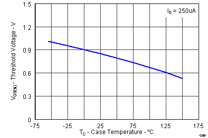
| VGS(th) | Gate-to-source threshold voltage | VDS = VGS, ID = 250 μA | 0.65 | 0.8 | 1.1 | V |
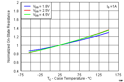
| RDS(on) | Drain-to-source on resistance | VGS = 1.8 V, ID = 1 A | 38 | 53 | mΩ | |
| VGS = 2.5 V, ID = 1 A | 29 | 39 | ||||
| VGS = 4.5 V, ID = 1 A | 26 | 34 | ||||
| gfs | Transconductance | VDS = 6 V, ID = 1 A | 23 | S | ||
| DYNAMIC CHARACTERISTICS | ||||||
| CISS | Input capacitance | VGS = 0 V, VDS = 6 V, ƒ = 1 MHz | 385 | 462 | pF | |
| COSS | Output capacitance | 245 | 294 | pF | ||
| CRSS | Reverse transfer capacitance | 18.1 | 22.6 | pF | ||
| Rg | Series gate resistance | 3 | Ω | |||
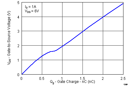
| Qg | Gate charge total (4.5 V) | VDS = 6 V, ID = 1 A | 2.3 | 2.9 | nC | |
| Qgd | Gate charge gate-to-drain | 0.3 | nC | |||
| Qgs | Gate charge gate-to-source | 0.5 | nC | |||
| Qg(th) | Gate charge at Vth | 0.3 | nC | |||
| QOSS | Output charge | VDS = 6.0 V, VGS = 0 V | 1.8 | nC | ||
| td(on) | Turn on delay time | VDS = 6 V, VGS = 4.5 V, ID = 1 A RG = 20 Ω |
3.9 | ns | ||
| tr | Rise time | 5.9 | ns | |||
| td(off) | Turn off delay time | 14.4 | ns | |||
| tf | Fall time | 9.7 | ns | |||
| DIODE CHARACTERISTICS | ||||||
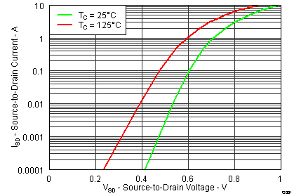
| VSD | Diode forward voltage | IS = 1 A, VGS = 0 V | 0.7 | 1 | V | |
| Qrr | Reverse recovery charge | VDS= 6 V, IS = 1 A, di/dt = 100 A/μs | 2.4 | nC | ||
| trr | Reverse recovery time | 11.5 | ns | |||
5.2 Thermal Information
(TA = 25°C unless otherwise stated)| THERMAL METRIC | MIN | TYP | MAX | UNIT | |
|---|---|---|---|---|---|
| RθJA | Thermal resistance junction-to-ambient (minimum Cu area) | 228.6 | °C/W | ||
| RθJA | Thermal resistance junction-to-ambient (1 in2 Cu area) | 131.1 | °C/W | ||
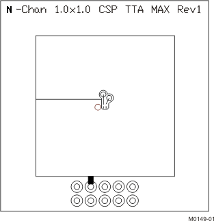 |
Max RθJA = 131.1°C/W when mounted on 1 inch2 of 2 oz. Cu. |
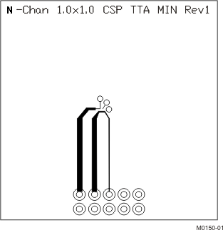 |
Max RθJA = 228.6°C/W when mounted on minimum pad area of 2 oz. Cu. |
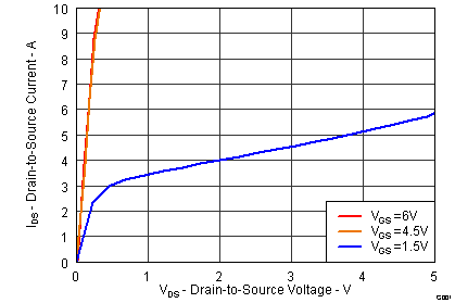
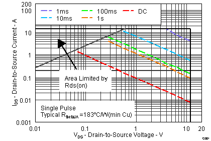
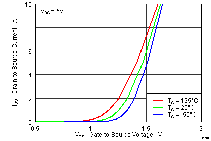
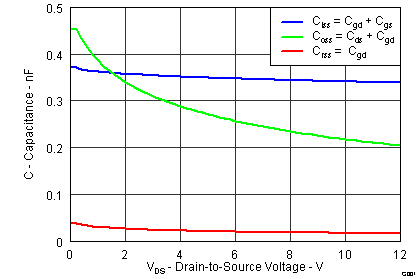
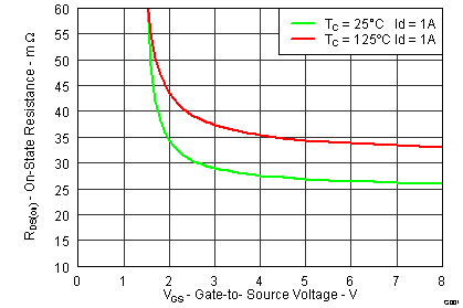
5.3 Typical MOSFET Characteristics
TA = 25°C (unless otherwise noted)
