SLPS247E December 2009 – August 2014 CSD16340Q3
PRODUCTION DATA.
- 1Features
- 2Applications
- 3Description
- 4Revision History
- 5Specifications
- 6Device and Documentation Support
- 7Mechanical, Packaging, and Orderable Information
Package Options
Refer to the PDF data sheet for device specific package drawings
Mechanical Data (Package|Pins)
- DQG|8
Thermal pad, mechanical data (Package|Pins)
Orderable Information
1 Features
- Optimized for 5 V Gate Drive
- Resistance Rated at VGS =2.5 V
- Ultra-Low Qg and Qgd
- Low Thermal Resistance
- Avalanche Rated
- Pb Free Terminal Plating
- RoHS Compliant
- Halogen Free
- SON 3.3-mm × 3.3-mm Plastic Package
2 Applications
- Point of Load Synchronous Buck Converter for Applications in Networking, Telecom, and Computing Systems
- Optimized for Control or Synchronous FET Applications
3 Description
This 25 V, 3.8 mΩ, 3.3 × 3.3 mm SON NexFET™ power MOSFET is designed to minimize losses in power conversion and optimized for 5 V gate drive applications.
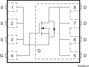
Top View
Product Summary
Ordering Information(1)
| Device | Media | Qty | Package | Ship |
|---|---|---|---|---|
| CSD16340Q3 | 13-Inch Reel | 2500 | SON 3.3 x 3.3 mm Plastic Package | Tape and Reel |
| CSD16340Q3T | 7-Inch Reel | 250 |
- For all available packages, see the orderable addendum at the end of the data sheet.
Absolute Maximum Ratings
| TA = 25°C | VALUE | UNIT | |
|---|---|---|---|
| VDS | Drain-to-Source Voltage | 25 | V |
| VGS | Gate-to-Source Voltage | +10 / –8 | V |
| ID | Continuous Drain Current, TC = 25°C | 60 | A |
| Continuous Drain Current(1) | 21 | A | |
| IDM | Pulsed Drain Current, TA = 25°C(2) | 115 | A |
| PD | Power Dissipation(1) | 3 | W |
| TJ, Tstg |
Operating Junction and Storage Temperature Range |
–55 to 150 | °C |
| EAS | Avalanche Energy, single pulse ID = 40 A, L = 0.1 mH, RG = 25 Ω |
80 | mJ |
- Typical RθJA = 39°C/W on 1in2 Cu (2 oz.) on 0.060" thick FR4 PCB.
- Pulse width ≤300 μs, duty cycle ≤2%
RDS(on) vs VGS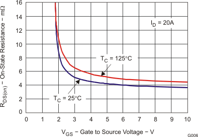 |
Gate Charge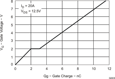 |