SLAS646C December 2009 – May 2015 DAC3282
PRODUCTION DATA.
- 1 Features
- 2 Applications
- 3 Description
- 4 Revision History
- 5 Pin Configuration and Functions
-
6 Specifications
- 6.1 Absolute Maximum Ratings
- 6.2 ESD Ratings
- 6.3 Recommended Operating Conditions
- 6.4 Thermal Information
- 6.5 Electrical Characteristics - DC Specifications
- 6.6 Electrical Characteristics - AC Specifications
- 6.7 Electrical Characteristics - Digital Specifications
- 6.8 Timing Characteristics
- 6.9 Typical Characteristics
-
7 Detailed Description
- 7.1 Overview
- 7.2 Functional Block Diagram
- 7.3
Feature Description
- 7.3.1 Input FIFO
- 7.3.2 FIFO Alarms
- 7.3.3 FIFO Modes of Operation
- 7.3.4 Dual Sync Sources Mode
- 7.3.5 Single Sync Source Mode
- 7.3.6 Bypass Mode
- 7.3.7 Data Pattern Checker
- 7.3.8 FIR Filters
- 7.3.9 Coarse Mixer
- 7.3.10 Digital Offset Control
- 7.3.11 Temperature Sensor
- 7.3.12 Sleep Modes
- 7.3.13 Reference Operation
- 7.4 Device Functional Modes
- 7.5 Programming
- 7.6
Register Maps
- 7.6.1 CONFIG0 (address = 0x00) [reset = 0x70]
- 7.6.2 CONFIG1 (address = 0x01) [reset = 0x11]
- 7.6.3 CONFIG2 (address = 0x02) [reset = 0x00]
- 7.6.4 CONFIG3 (address = 0x03) [reset = 0x10]
- 7.6.5 CONFIG4 (address = 0x04) [reset = 0xFF]
- 7.6.6 CONFIG5 (address = 0x05) READ ONLY
- 7.6.7 CONFIG6 (address =0x06) [reset = 0x00]
- 7.6.8 CONFIG7 (address = 0x07) [reset = 0x00] (WRITE TO CLEAR)
- 7.6.9 CONFIG8 (address = 0x08) [reset = 0x00] (WRITE TO CLEAR)
- 7.6.10 CONFIG9 (address = 0x09) [reset = 0x7A]
- 7.6.11 CONFIG10 (address = 0x0A) [reset = 0xB6]
- 7.6.12 CONFIG11 (address = 0x0B) [reset = 0xEA]
- 7.6.13 CONFIG12 (address =0x0C) [reset = 0x45]
- 7.6.14 CONFIG13 (address =0x0D) [reset = 0x1A]
- 7.6.15 CONFIG14 Register Name (address = 0x0E) [reset = 0x16]
- 7.6.16 CONFIG15 Register Name (address = 0x0F) [reset = 0xAA]
- 7.6.17 CONFIG16 (address = 0x10) [reset = 0xC6]
- 7.6.18 CONFIG17 (address = 0x11) [reset = 0x00]
- 7.6.19 CONFIG18 (address = 0x12) [reset = 0x02]
- 7.6.20 CONFIG19 (address = 0x13) [reset = 0x00]
- 7.6.21 CONFIG20 (address = 0x14) [reset = 0x00] (CAUSES AUTOSYNC)
- 7.6.22 CONFIG21 (address = 0x15) [reset = 0x00]
- 7.6.23 CONFIG22 (address = 0x16) [reset = 0x00]
- 7.6.24 CONFIG23 (address = 0x17) [reset = 0x00]
- 7.6.25 CONFIG24 (address = 0x18) [reset = 0x83]
- 7.6.26 CONFIG25 (address = 0x19) [reset = 0x00]
- 7.6.27 CONFIG26 (address = 0x1A) [reset = 0x00]
- 7.6.28 CONFIG27 (address =0x1B) [reset = 0x00]
- 7.6.29 CONFIG28 (address = 0x1C) [reset = 0x00]
- 7.6.30 CONFIG29 (address = 0x1D) [reset = 0x00]
- 7.6.31 CONFIG30 (address = 0x1E) [reset = 0x00]
- 7.6.32 VERSION31 (address = 0x1F) [reset = 0x43] (READ ONLY)
- 8 Application and Implementation
- 9 Power Supply Recommendations
- 10Layout
- 11Device and Documentation Support
- 12Mechanical, Packaging, and Orderable Information
Package Options
Mechanical Data (Package|Pins)
- RGZ|48
Thermal pad, mechanical data (Package|Pins)
- RGZ|48
Orderable Information
10 Layout
10.1 Layout Guidelines
The design of the PCB is critical to achieve the full performance of the DAC3282 device. Defining the PCB stackup should be the first step in the board design. Experience has shown that at least 6 layers are required to adequately route all required signals to and from the device. Each signal routing layer must have an adjacent solid ground plane to control signal return paths to have minimal loop areas and to achieve controlled impedances for microstrip and stripline routing. Power planes must also have adjacent solid ground planes to control supply return paths. Minimizing the spacing between supply and ground planes improves performance by increasing the distributed decoupling.
Although the DAC3282 device consists of both analog and digital circuitry, TI highly recommends solid ground planes that encompass the device and its input and output signal paths. TI does not recommend split ground planes that divide the analog and digital portions of the device. Split ground planes may improve performance if a nearby, noisy, digital device is corrupting the ground reference of the analog signal path. When split ground planes are employed, one must carefully control the supply return paths and keep the paths on top of their respective ground reference planes.
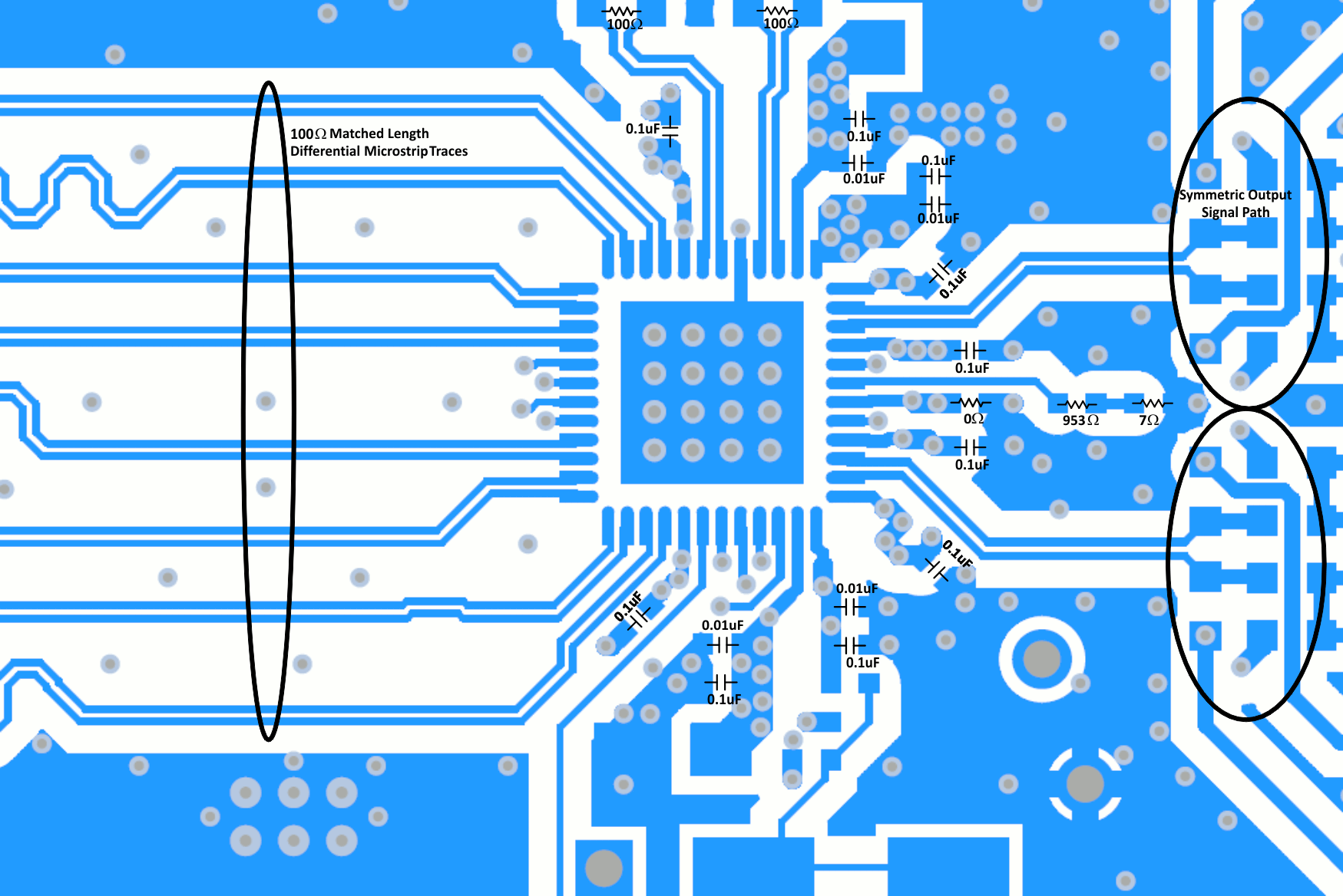
Quality analog output signals and input conversion clock signal path layout is required for full dynamic performance. Symmetry of the differential signal paths and discrete components in the path is mandatory and symmetrical shunt-oriented components should have a common grounding via. The high frequency requirements of the analog output and clock signal paths necessitate using differential routing with controlled impedances and minimizing signal path stubs (including vias) when possible.
Coupling onto or between the clock and output signal paths should be avoided using any isolation techniques available including distance isolation, orientation planning to prevent field coupling of components like inductors and transformers, and providing well coupled reference planes. Via stitching around the clock signal path and the input analog signal path provides a quiet ground reference for the critical signal paths and reduces noise coupling onto these paths. Sensitive signal traces must not cross other signal traces or power routing on adjacent PCB layers, rather a ground plane must separate the traces. If necessary, the traces should cross at 90 ° angles to minimize crosstalk.
The substrate (dielectric) material requirements of the PCB are largely influenced by the speed and length of the high speed serial lanes. Affordable and common FR4 varieties are adequate in most cases.
Coupling of ambient signals into the signal path is reduced by providing quiet, close reference planes and by maintaining signal path symmetry to ensure the coupled noise is common-mode. Faraday caging may be used in very noisy environments and high dynamic range applications to isolate the signal path.
10.2 Layout Example
 Figure 93. Layout Example