SLAS693C March 2010 – March 2015 DAC3283
PRODUCTION DATA.
- 1 Features
- 2 Applications
- 3 Description
- 4 Simplified Schematic
- 5 Revision History
- 6 Pin Configuration and Functions
-
7 Specifications
- 7.1 Absolute Maximum Ratings
- 7.2 ESD Ratings
- 7.3 Recommended Operating Conditions
- 7.4 Thermal Information
- 7.5 Electrical Characteristics - DC Specifications
- 7.6 Electrical Characteristics - AC Specifications
- 7.7 Electrical Characteristics - Digital Specifications
- 7.8 Timing Requirements
- 7.9 Typical Characteristics
-
8 Detailed Description
- 8.1 Overview
- 8.2 Functional Block Diagram
- 8.3
Feature Description
- 8.3.1
Definition Of Specifications
- 8.3.1.1 Adjacent Carrier Leakage Ratio (ACLR)
- 8.3.1.2 Analog and Digital Power Supply Rejection Ratio (APSSR, DPSSR)
- 8.3.1.3 Differential Nonlinearity (DNL)
- 8.3.1.4 Gain Drift
- 8.3.1.5 Gain Error
- 8.3.1.6 Integral Nonlinearity (INL)
- 8.3.1.7 Intermodulation Distortion (IMD3, IMD)
- 8.3.1.8 Offset Drift
- 8.3.1.9 Offset Error
- 8.3.1.10 Output Compliance Range
- 8.3.1.11 Reference Voltage Drift
- 8.3.1.12 Spurious Free Dynamic Range (SFDR)
- 8.3.1.13 Noise Spectral Density (NSD)
- 8.3.1
Definition Of Specifications
- 8.4
Device Functional Modes
- 8.4.1 Serial Interface
- 8.4.2 Data Interface
- 8.4.3 Input FIFO
- 8.4.4 FIFO Alarms
- 8.4.5 FIFO Modes of Operation
- 8.4.6 Multi-Device Operation
- 8.4.7 Data Pattern Checker
- 8.4.8 DATACLK Monitor
- 8.4.9 FIR Filters
- 8.4.10 Coarse Mixer
- 8.4.11 Quadrature Modulation Correction (QMC)
- 8.4.12 Digital Offset Control
- 8.4.13 Temperature Sensor
- 8.4.14 Sleep Modes
- 8.4.15 LVPECL Inputs
- 8.4.16 LVDS INPUTS
- 8.4.17 CMOS Digital Inputs
- 8.4.18 Reference Operation
- 8.4.19 DAC Transfer Function
- 8.4.20 Analog Current Outputs
- 8.4.21 Passive Interface to Analog Quadrature Modulators
- 8.5
Register Maps
- 8.5.1 CONFIG0 (address = 0x00) [reset = 0x70]
- 8.5.2 CONFIG1 (address = 0x01) [reset = 0x11]
- 8.5.3 CONFIG2 (address = 0x02) [reset = 0x00]
- 8.5.4 CONFIG3 (address = 0x03) [reset = 0x10]
- 8.5.5 CONFIG4 (address = 0x04) [reset = 0xFF]
- 8.5.6 CONFIG5 (address = 0x05) READ ONLY
- 8.5.7 CONFIG6 (address =0x06) [reset = 0x00]
- 8.5.8 CONFIG7 (address = 0x07) [reset = 0x00] (WRITE TO CLEAR)
- 8.5.9 CONFIG8 (address = 0x08) [reset = 0x00] (WRITE TO CLEAR)
- 8.5.10 CONFIG9 (address = 0x09) [reset = 0x7A]
- 8.5.11 CONFIG10 (address = 0x0A) [reset = 0xB6]
- 8.5.12 CONFIG11 (address = 0x0B) [reset = 0xEA]
- 8.5.13 CONFIG12 (address =0x0C) [reset = 0x45]
- 8.5.14 CONFIG13 (address =0x0D) [reset = 0x1A]
- 8.5.15 CONFIG14 Register Name (address = 0x0E) [reset = 0x16]
- 8.5.16 CONFIG15 Register Name (address = 0x0F) [reset = 0xAA]
- 8.5.17 CONFIG16 (address = 0x10) [reset = 0xV6]
- 8.5.18 CONFIG17 (address = 0x11) [reset = 0x24]
- 8.5.19 CONFIG18 (address = 0x12) [reset = 0x02]
- 8.5.20 CONFIG19 (address = 0x13) [reset = 0x00]
- 8.5.21 CONFIG20 (address = 0x14) [reset = 0x00] (CAUSES AUTOSYNC)
- 8.5.22 CONFIG21 (address = 0x15) [reset = 0x00]
- 8.5.23 CONFIG22 (address = 0x16) [reset = 0x00]
- 8.5.24 CONFIG23 (address = 0x17) [reset = 0x00]
- 8.5.25 CONFIG24 (address = 0x18) [reset = 0x83]
- 8.5.26 CONFIG25 (address = 0x19) [reset = 0x00]
- 8.5.27 CONFIG26 (address = 0x1a) [reset = 0x00]
- 8.5.28 CONFIG27 (address =0x1b) [reset = 0x00] (CAUSES AUTOSYNC)
- 8.5.29 CONFIG28 (address = 0x1C) [reset = 0x00]
- 8.5.30 CONFIG29 (address = 0x1D) [reset = 0x00]
- 8.5.31 CONFIG30 (address = 0x1E) [reset = 0x24]
- 8.5.32 VERSION31 (address = 0x1F) [reset = 0x12] (PARTIAL READ ONLY)
- 9 Application and Implementation
- 10Power Supply Recommendations
- 11Layout
- 12Device and Documentation Support
- 13Mechanical, Packaging, and Orderable Information
Package Options
Mechanical Data (Package|Pins)
- RGZ|48
Thermal pad, mechanical data (Package|Pins)
- RGZ|48
Orderable Information
8 Detailed Description
8.1 Overview
The DAC3283 is a dual-channel 16-bit 800 MSPS digital-to-analog converter (DAC) with an 8-bit LVDS input data bus with on-chip termination, optional 2x-4x interpolation filters, digital IQ compensation and internal voltage reference. Input data can be interpolated by 2x or 4x through on-chip interpolating FIR filters with over 85 dB of stop-band attenuation. Multiple DAC3283 devices can be fully synchronized. The DAC3283 allows either a complex or real output. An optional coarse mixer in complex mode provides frequency upconversion and the dual DAC output produces a complex Hilbert Transform pair. The digital IQ compensation feature allows optimization of phase, gain and offset to maximize sideband rejection and minimize LO feed-through of an external quadrature modulator performing the final single sideband RF up-conversion.
8.2 Functional Block Diagram
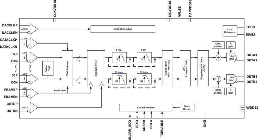
8.3 Feature Description
8.3.1 Definition Of Specifications
8.3.1.1 Adjacent Carrier Leakage Ratio (ACLR)
Defined for a 3.84Mcps 3GPP W-CDMA input signal measured in a 3.84MHz bandwidth at a 5MHz offset from the carrier with a 12dB peak-to-average ratio.
8.3.1.2 Analog and Digital Power Supply Rejection Ratio (APSSR, DPSSR)
Defined as the percentage error in the ratio of the delta IOUT and delta supply voltage normalized with respect to the ideal IOUT current.
8.3.1.3 Differential Nonlinearity (DNL)
Defined as the variation in analog output associated with an ideal 1 LSB change in the digital input code.
8.3.1.4 Gain Drift
Defined as the maximum change in gain, in terms of ppm of full-scale range (FSR) per °C, from the value at ambient (25°C) to values over the full operating temperature range.
8.3.1.5 Gain Error
Defined as the percentage error (in FSR%) for the ratio between the measured full-scale output current and the ideal full-scale output current.
8.3.1.6 Integral Nonlinearity (INL)
Defined as the maximum deviation of the actual analog output from the ideal output, determined by a straight line drawn from zero scale to full scale.
8.3.1.7 Intermodulation Distortion (IMD3, IMD)
The two-tone IMD3 or four-tone IMD is defined as the ratio (in dBc) of the worst 3rd-order (or higher) intermodulation distortion product to either fundamental output tone.
8.3.1.8 Offset Drift
Defined as the maximum change in DC offset, in terms of ppm of full-scale range (FSR) per °C, from the value at ambient (25°C) to values over the full operating temperature range.
8.3.1.9 Offset Error
Defined as the percentage error (in FSR%) for the ratio between the measured mid-scale output current and the ideal mid-scale output current.
8.3.1.10 Output Compliance Range
Defined as the minimum and maximum allowable voltage at the output of the current-output DAC. Exceeding this limit may result reduced reliability of the device or adversely affecting distortion performance.
8.3.1.11 Reference Voltage Drift
Defined as the maximum change of the reference voltage in ppm per degree Celsius from value at ambient (25°C) to values over the full operating temperature range.
8.3.1.12 Spurious Free Dynamic Range (SFDR)
Defined as the difference (in dBc) between the peak amplitude of the output signal and the peak spurious signal.
8.4 Device Functional Modes
8.4.1 Serial Interface
The serial port of the DAC3283 is a flexible serial interface which communicates with industry standard microprocessors and microcontrollers. The interface provides read/write access to all registers used to define the operating modes of DAC3283. It is compatible with most synchronous transfer formats and can be configured as a 3 or 4 pin interface by sif4_ena in register CONFIG23. In both configurations, SCLK is the serial interface input clock and SDENB is serial interface enable. For 3 pin configuration, SDIO is a bidirectional pin for both data in and data out. For 4 pin configuration, SDIO is bidirectional and ALARM_SDO is data out only. Data is input into the device with the rising edge of SCLK. Data is output from the device on the falling edge of SCLK.
Each read/write operation is framed by signal SDENB (Serial Data Enable Bar) asserted low for 2 to 5 bytes, depending on the data length to be transferred (1–4 bytes). The first frame byte is the instruction cycle which identifies the following data transfer cycle as read or write, how many bytes to transfer, and what address to transfer the data. Table 1 indicates the function of each bit in the instruction cycle and is followed by a detailed description of each bit. Frame bytes 2 to 5 comprise the data transfer cycle.
Table 1. Instruction Byte of the Serial Interface
| MSB | LSB |
| Bit | 7 | 6 | 5 | 4 | 3 | 2 | 1 | 0 |
| Description | R/W | N1 | N0 | A4 | A3 | A2 | A1 | A0 |
| R/W | Identifies the following data transfer cycle as a read or write operation. A high indicates a read operation from DAC3283 and a low indicates a write operation to DAC3283. | ||
| [N1:N0] | Identifies the number of data bytes to be transferred per Table 2. Data is transferred MSB first. | ||
Table 2. Number of Transferred Bytes Within One Communication Frame
| N1 | N0 | Description |
|---|---|---|
| 0 | 0 | Transfer 1 Byte |
| 0 | 1 | Transfer 2 Bytes |
| 1 | 0 | Transfer 3 Bytes |
| 1 | 1 | Transfer 4 Bytes |
| [A4:A0] | Identifies the address of the register to be accessed during the read or write operation. For multi-byte transfers, this address is the starting address. Note that the address is written to the DAC3283 MSB first and counts down for each byte. | ||
Figure 26 shows the serial interface timing diagram for a DAC3283 write operation. SCLK is the serial interface clock input to DAC3283. Serial data enable SDENB is an active low input to DAC3283. SDIO is serial data in. Input data to DAC3283 is clocked on the rising edges of SCLK.
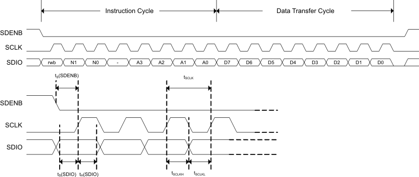 Figure 26. Serial Interface Write Timing Diagram
Figure 27 shows the serial interface timing diagram for a DAC3283 read operation. SCLK is the serial interface clock input to DAC3283. Serial data enable SDENB is an active low input to DAC3283. SDIO is serial data in during the instruction cycle. In 3 pin configuration, SDIO is data out from DAC3283 during the data transfer cycle(s), while ALARM_SDO is in a high-impedance state. In 4 pin configuration, both ALARM_SDO and SDIO are data out from DAC3283 during the data transfer cycle(s). At the end of the data transfer, ALARM_SDO will output low on the final falling edge of SCLK until the rising edge of SDENB when it will 3-state.
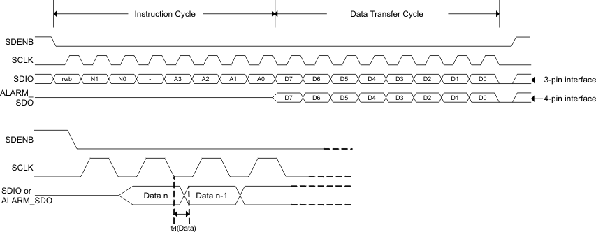 Figure 27. Serial Interface Read Timing Diagram
8.4.2 Data Interface
The DAC3283 has a single 8-bit LVDS bus that accepts dual, 16-bit data input in byte-wide format. Data into the DAC3283 is formatted according to the diagram shown in Figure 28 where index 0 is the data LSB and index 15 is the data MSB. The data is sampled by DATACLK, a double data rate (DDR) clock.
The FRAME signal is required to indicate the beginning of a frame. The frame signal can be either a pulse or a periodic signal where the frame period corresponds to 8 samples. The pulse-width (t(FRAME)) needs to be at least equal to ½ of the DATACLK period. FRAME is sampled by a rising edge in DATACLK.
The setup and hold requirements listed in the specifications tables must be met to ensure proper sampling.
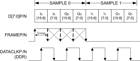 Figure 28. Byte-Wide Data Transmission Format
8.4.3 Input FIFO
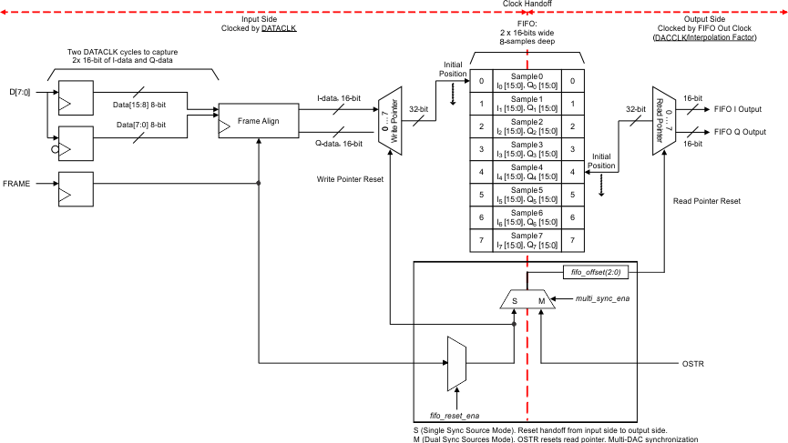
The DAC3283 includes a 2-channel, 16-bits wide and 8-samples deep input FIFO which acts as an elastic buffer. The purpose of the FIFO is to absorb any timing variations between the input data and the internal DAC data rate clock such as the ones resulting from clock-to-data variations from the data source.
Figure 29 shows a simplified block diagram of the FIFO.
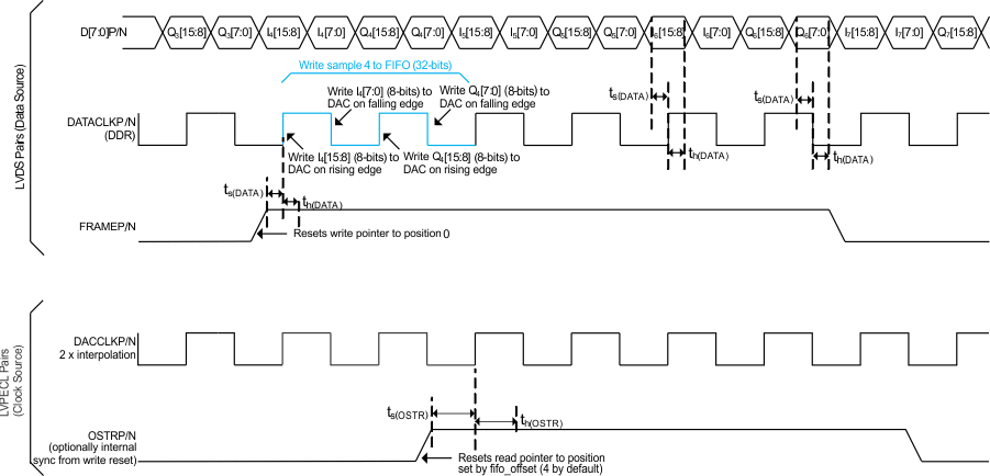
Data is written to the device 8-bits at a time on the rising and falling edges of DATACLK. In order to form a complete 32-bit wide sample (16-bit I-data and 16-bit Q-data) two DATACLK periods are required as shown in Figure 30. Each 32-bit wide sample is written into the FIFO at the address indicated by the write pointer. Similarly, data from the FIFO is read by the FIFO Out Clock 32-bits at a time from the address indicated by the read pointer. The FIFO Out Clock is generated internally from the DACCLK signal and its rate is equal to DACCLK/Interpolation. Each time a FIFO write or FIFO read is done the corresponding pointer moves to the next address.
The reset position for the FIFO read and write pointers is set by default to addresses 0 and 4 as shown in Figure 29. This offset gives optimal margin within the FIFO. The default read pointer location can be set to another value using fifo_offset(2:0) in register CONFIG3. Under normal conditions data is written-to and read-from the FIFO at the same rate and consequently the write and read pointer gap remains constant. If the FIFO write and read rates are different, the corresponding pointers will be cycling at different speeds which could result in pointer collision. Under this condition the FIFO attempts to read and write data from the same address at the same time which will result in errors and thus must be avoided.
The FRAME signal besides acting as a frame indicator can also used to reset the FIFO pointers to their initial location. Unlike Data, the FRAME signal is latched only on the rising edges of DATACLK. When a rising edge occurs on FRAME, the pointers will return to their original position. The write pointer is always set back to position 0 upon reset. The read pointer reset position is determined by fifo_offset (address 4 by default).
Similarly, the read pointer sync source is selected by multi_sync_sel (CONFIG19). Either the FRAME or OSTR signal can be set to reset the read pointer. If FRAME is used to reset the read pointer, the FIFO Out Clock will recapture the FRAME signal to reset the read pointer. This clock domain transfer (DATACLK to FIFO Out Clock) results in phase ambiguity of the reset signal. This limits the precise control of the output timing and makes full synchronization of multiple devices difficult.
To alleviate this, the device offers the alternative of resetting the FIFO read pointer independently of the write pointer by using the OSTR signal. The OSTR signal is sampled by DACCLK and must satisfy the timing requirements in the specification table. In order to minimize the skew it is recommended to use the same clock distribution device such as Texas Instruments CDCE62005 to provide the DACCLK and OSTR signals to all the DAC3283 devices in the system. Swapping the polarity of the DACCLK output with respect to the OSTR output establishes proper phase relationship.
The FIFO pointers reset procedure can be done periodically or only once during initialization as the pointers automatically return to the initial position when the FIFO has been filled. To reset the FIFO periodically, it is necessary to have FRAME and OSTR signals to repeat at multiple of 8 FIFO samples. To disable FIFO reset, set fifo_reset_ena and multi_sync_ena (CONFIG0) to 0.
The frequency limitation for the FRAME signal is the following:
fSYNC = fDATACLK/(n x 16) where n = 1, 2, ...
The frequency limitation for the OSTR signal is the following:
fOSTR = fDAC/(n x interpolation x 8) where n = 1, 2, ...
The frequencies above are at maximum when n = 1. This is when FRAME and OSTR have a rising edge transition every 8 FIFO samples. The occurrence can be made less frequently by setting n > 1, for example, every n x 8 FIFO samples.
8.4.4 FIFO Alarms
The FIFO only operates correctly when the write and read pointers are positioned properly. If either pointer over or under runs the other, samples will be duplicated or skipped. To prevent this, register CONFIG7 can be used to track three FIFO related alarms:
- alarm_fifo_2away. Occurs when the pointers are within two addresses of each other.
- alarm_fifo_1away. Occurs when the pointers are within one address of each other.
- alarm_fifo_collision. Occurs when the pointers are equal to each other.
These three alarm events are generated asynchronously with respect to the clocks and can be accessed either through CONFIG7 or through the ALARM_SDO pin.
8.4.5 FIFO Modes of Operation
The DAC3283 FIFO can be completely bypassed through registers config0 and config19. The register configuration for each mode is described in Table 3.
| Register | Control Bits |
| config0 | fifo_ena, fifo_reset_ena, multi_sync_ena |
| config19 | multi_sync_sel |
Table 3. FIFO Operation Modes
| Config1 FIFO Bits | Config19 | |||
|---|---|---|---|---|
| FIFO Mode | fifo_ena | fifo_reset_ena | multi_sync_ena | multi_sync_sel |
| Dual Sync Sources | 1 | 1 | 1 | 0 |
| Single Sync Source | 1 | 1 | 1 | 1 |
| Bypass | 0 | X | X | X |
8.4.5.1 Dual Sync Souces Mode
This is the recommended mode of operation for those applications that require precise control of the output timing. In Dual Sync Sources mode, the FIFO write and read pointers are reset independently. The FIFO write pointer is reset using the LVDS FRAME signal, and the FIFO read pointer is reset using the LVPECL OSTR signal. This allows LVPECL OSTR signal to control the phase of the output for either a single chip or multiple chips. Multiple devices can be fully synchronized in this mode.
8.4.5.2 Single Sync Source Mode
In Single Sync Source mode, the FIFO write and read pointers are reset from the LVDS FRAME signal. This mode has a possibility of up to 2 DAC clocks offset between the outputs of multiple devices (The DAC outputs of the same device maintain the same phase). Applications requiring exact output timing control will need Dual Sync Sources mode instead of Single Sync Source mode. A rising edge for FIFO and clock divider sync is recommended. Periodic sync signal is not recommended due to non-deterministic latency of the sync signal through the clock domain transfer.
8.4.5.3 Bypass Mode
In FIFO bypass mode, the FIFO block is not used. As a result the input data is handed off from the DATACLK to the DACCLK domain without any compensation. In this mode the relationship between DATACLK and DACCLK (t_align) is critical and used as a synchronizing mechanism for the internal logic. Due to the t_align constraint it is highly recommended that a clock synchronizer device such as Texas Instruments’ CDCM7005 or CDCE62005 is used to provide both clock inputs. In bypass mode the pointers have no effect on the data path or handoff.
8.4.6 Multi-Device Operation
In various applications, such as multi antenna systems where the various transmit channels information is correlated, it is required that multiple DAC devices are completely synchronized such that their outputs are phase aligned. The DAC3283 architecture supports this mode of operation.
8.4.6.1 Multi-Device Synchronization: Dual Sync Sources Mode
For single or multi-device synchronization it is important that delay differences in the data are absorbed by the device so that latency through the device remains the same. Furthermore, to guarantee that the outputs from each DAC are phase aligned it is necessary that data is read from the FIFO of each device simultaneously. In the DAC3283 this is accomplished by operating the multiple devices in Dual Sync Sources mode. In this mode the additional OSTR signal is required by each DAC3283 to be synchronized.
Data into the device is input as LVDS signals from one or multiple baseband ASICs or FPGAs. Data into the multiple DAC devices can experience different delays due to variations in the digital source output paths or board level wiring. These different delays can be effectively absorbed by the DAC3283 FIFO so that all outputs are phase aligned correctly.
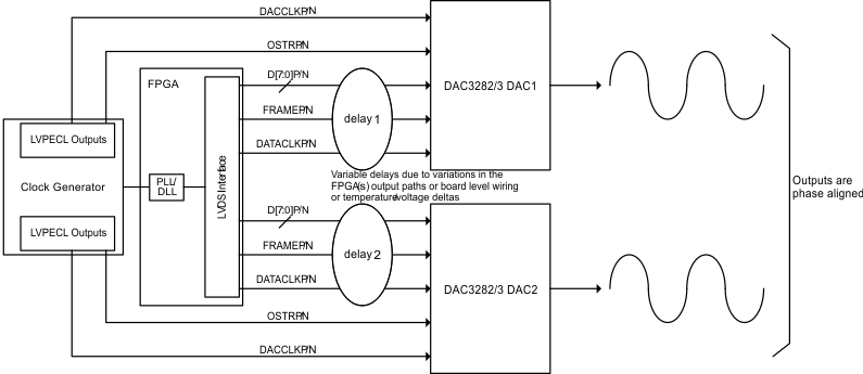 Figure 31. Synchronization System in Dual Sync Sources Mode
For correct operation both OSTR and DACCLK must be generated from the same clock domain. The OSTR signal is sampled by DACCLK and must satisfy the timing requirements in the specifications table. If the clock generator does not have the ability to delay the DACCLK to meet the OSTR timing requirement, the polarity of the DACCLK outputs can be swapped with respect to the OSTR ones to create 180 degree phase delay of the DACCLK. This may help establish proper setup and hold time requirement of the OSTR signal.
Careful board layout planning must be done to ensure that the DACCLK and OSTR signals are distributed from device to device with the lowest skew possible as this will affect the synchronization process. In order to minimize the skew across devices it is recommended to use the same clock distribution device to provide the DACCLK and OSTR signals to all the DAC devices in the system.
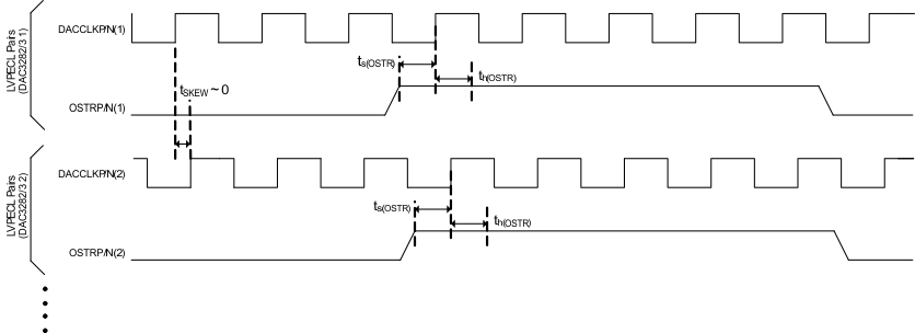 Figure 32. Timing Diagram for LVPECL Synchronization Signals
The following steps are required to ensure the devices are fully synchronized. The procedure assumes all the DAC3283 devices have a DACCLK and OSTR signal and the following steps must be carried out on each device.
- Start-up the device as described in the power-up sequence. Set the DAC3283 in Dual Sync Sources mode and select OSTR as the FIFO output pointer sync source and clock divider sync source (multi_sync_sel in register config19).
- Sync the clock divider and FIFO pointers.
- Verify there are no FIFO alarms either through register config7 or through the ALARM_SDO pin.
After these steps all the DAC3283 outputs will be synchronized.
8.4.6.2 Multi-Device Operation: Single Sync Source Mode
In Single Sync Source mode, the FIFO write and read pointers are reset from the same FRAME source. Although the FIFO in this mode can still absorb the data delay differences due to variations in the digital source output paths or board level wiring, it is impossible to guarantee data will be read from the FIFO of different devices simultaneously thus preventing exact phase alignment.
The FIFO read pointer reset is handoff between the two clock domains (DATACLK and FIFO OUT CLOCK) by simply re-sampling the write pointer reset. Since the two clocks are asynchronous there is a small but distinct possibility of a meta-stablility during the pointer handoff. This meta-stability can cause the outputs of the multiple devices to slip by up to 2 DAC clock cycles.
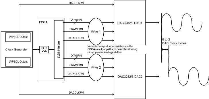 Figure 33. Multi-Device Operation in Single Sync Source Mode
8.4.7 Data Pattern Checker
The DAC3283 incorporates a simple pattern checker test in order to determine errors in the data interface. The main cause of failures is setup/hold timing issues. The test mode is enabled by asserting iotest_ena in register config1. In test mode the analog outputs are deactivated regardless of the state of TXENABLE.
The data pattern key used for the test is 8 words long and is specified by the contents of iotest_pattern[0:7] in registers config9 through config16. The data pattern key can be modified by changing the contents of these registers.
The first word in the test frame is determined by a rising edge transition in FRAME. At this transition, the pattern0 word should be input to the data pins. Patterns 1 through 7 should follow sequentially on each edge of DATACLK (rising and falling). The sequence should be repeated until the pattern checker test is disabled by setting iotest_ena back to “0”. It is not necessary to have a rising FRAME edge aligned with every pattern0 word, just the first one to mark the beginning of the series.
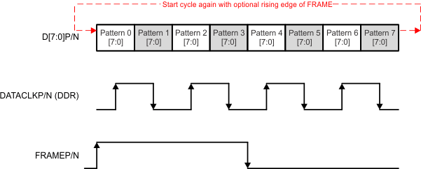 Figure 34. IO Pattern Checker Data Transmission Format
The test mode determines if the 8-bit LVDS data D[7:0]P/N of all the patterns were received correctly by comparing the received data against the data pattern key. If any of the 8-bit data D[7:0]P/N were received incorrectly, the corresponding bits in iotest_results(7:0) in register config8 will be set to “1” to indicate bit error location. Furthermore, the error condition will trigger the alarm_from_iotest bit in register config7 to indicate a general error in the data interface. When data pattern checker mode is enabled, this alarm in register config7, bit 3 is the only valid alarm. Other alarms in register config7 are not valid and can be disregarded.
For instance, pattern0 is programmed to the default of 0x7A. If the received Pattern 0 is 0x7B, then bit 0 in iotest_results(7:0) will be set to “1” to indicate an error in bit 0 location. The alarm_from_iotest will also be set to “1” to report the data transfer error. The user can then narrow down the error from the bit location information and implement the fix accordingly.
The alarms can be cleared by writing 0x00 to iotest_results(7:0) and "0" to alarm_from_iotest through the serial interface. The serial interface will read back 0s if there are no errors or if the errors are cleared. The corresponding alarm bit will remain a "1" if the errors remain.
It is recommended to enable the pattern checker and then run the pattern sequence for 100 or more complete cycles before clearing the iotest_results(7:0) and alarm_from_iotest. This will eliminate the possibility of false alarms generated during the setup sequence.
8.4.8 DATACLK Monitor
The DAC3283 incorporates a clock monitor to determine if DATACLK is present. A missing DATACLK may result in unexpected DAC outputs. As shown in Figure 36, the clock monitor circuit is a simple counter circuit. It is reset on each rising edge of DATACLK, and counts up with each rising edge of FIFOOUT_CLK. The output of the counter has two latches: clk_alarm latch and tx_off latch. If the missing DATACLK is registered by the clock monitor circuit after the counter reached the count of four, it will send a pulse to the two latches, which issue two alarms, respectively.
 Figure 36. DATACLK Monitor Circuit
| CIRCUIT | FUNCTIONS | REGISTER LOCATION | STATE | DESCRIPTION |
|---|---|---|---|---|
| clk_alarm latch | clk_alarm_mask | CONFIG17, bit4 read/write | 1 | masks the alarm signal to the CMOS ALARM_SDO |
| 0 | unmasks the alarm signal to the CMOS ALARM_SDO | |||
| clk_alarm_ena | CONFIG17, bit1 read/write | 1 | clears the latch and enables the clock loss monitoring | |
| 0 | holds the latch at reset at all times | |||
| clk_alarm | VERSION31, bit7 read-only | 1 | indicates clock loss event | |
| 0 | indicates normal operation | |||
| tx_off latch | tx_off_mask | CONFIG17, bit3 read/write | 1 | masks the alarm signal to the CMOS ALARM_SDO |
| 0 | unmasks the alarm signal to the CMOS ALARM_SDO | |||
| tx_off_ena | CONFIG17, bit0 read/write | 1 | clears the latch and enables the clock loss monitoring | |
| 0 | holds the latch at reset at all times | |||
| tx_off | VERSION31, bit6 read-only | 1 | indicates output disabled event | |
| 0 | indicates normal operation |
The purpose of the clk_alarm latch is to register the loss of DATACLK event. Upon the event, the latch will issue a read-only clk_alarm alarm. This latch can be held reset at all time by setting clk_alarm_ena = ‘0’ at all time.
The purpose of the tx_off latch is to disable the output when the DATACLK is lost. Upon the event, the latch will issue a read-only tx_off alarm. When this alarm is set, the DAC3283 outputs are automatically disabled by setting output data to mid-scale. This latch can be held reset at all time by setting tx_off_ena = ‘0’ at all time.
Both alarms are set by default to trigger the ALARM_SDO pin in 3-pin SPI mode. By writing clk_alarm_mask and tx_off_mask to ‘1’, the ALARM_SDO will ignore these two alarms. This may be useful if the ALARM_SDO is needed to report other critical alarms in the interrupt routine.
These two latches can be held reset at all times, effectively ignoring any clock monitor output, by setting clk_alarm_ena and tx_off_ena to ‘0”. When a ‘0’ is written to either of these two register bits, it will force the latch output low. For the latches to report an error, the clk_monitor_ena and tx_off_ena must be written to a ‘0’ and then a ‘1’.
The clock monitoring function is implemented as follows:
- Power up the device using the recommended power-up sequence.
- Configure the device using the SPI bus.
- Provide both the DATACLK and DACCLK.
- Reset the clock monitor circuit and the latches by writing clk_alarm_ena and tx_off_ena a ‘0”, and then ‘1’ in CONFIG17.
- Unmask the alarms by setting clk_alarm_mask and tx_off_mask to ‘0’ in CONFIG17.
If the DATACLK is interrupted, the ALARM_SDO pin will transition to indicate error. The interrupt service routine can check the following:
- Read clk_alarm and tx_off in CONFIG31 and other alarms in CONFIG7 to determine the error that triggered the alarm.
- If clk_alarm and tx_off alarms are set in CONFIG31, then DATACLK was interrupted and the DAC outputs should be set to mid-scale.
- Implement system check to recover the DATACLK.
- Reset the clock monitor circuit and clk_alarm latch by writing clk_alarm_ena a ‘0”, and then ‘1’ in CONFIG17.
- Read clk_alarm in CONFIG31 to verify if the clock loss event has not re-triggered the alarm.
- Once the clock monitor indicates the DATACLK is stable, resynchronize the FIFO. See Power-Up Sequence section for detail.
- Reset the transmit disable latch by writing tx_off_ena a ‘0”, and then ‘1’ in CONFIG17. This will re-enable the DAC to output actual data.
NOTE
The ALARM_SDO pin in 4-pin SPI mode functions as SPI register data output. The system will need to poll VERSION31 alarms frequently in order to detect the DATACLK interruption errors.
8.4.9 FIR Filters
Figure 37 and Figure 38 show the magnitude spectrum response for the FIR0 and FIR1 interpolating half-band filters where fIN is the input data rate to the FIR filter. Figure 39 and Figure 40 show the composite filter response for 2x and 4x interpolation. The transition band for all the interpolation settings is from 0.4 to 0.6 x fDATA (the input data rate to the device) with < 0.002dB of pass-band ripple and > 85dB stop-band attenuation.
The filter taps for all digital filters are listed in Table 4.
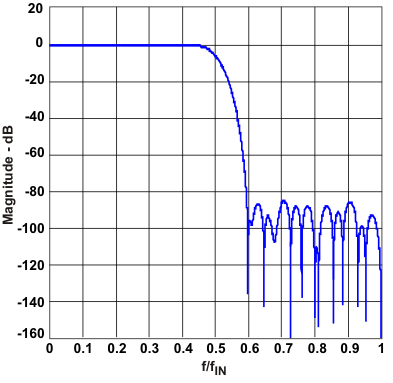 Figure 37. Magnitude Spectrum for FIR0
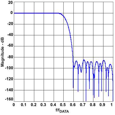 Figure 39. 2x Interpolation Composite Response
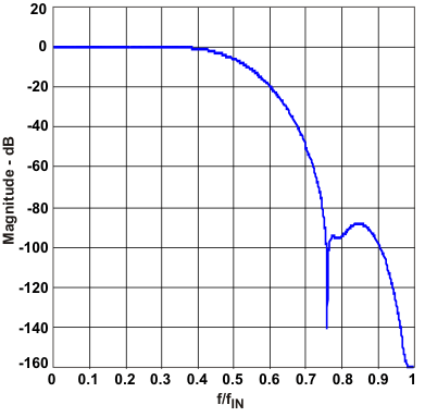 Figure 38. Magnitude Spectrum for FIR1
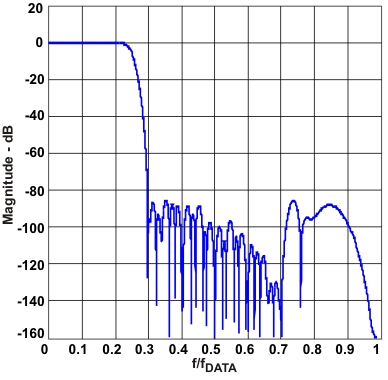 Figure 40. 4x Interpolation Composite Response
Table 4. FIR Filter Coefficients
| FIR0 2x Interpolating Half-band Filter |
FIR1 2x Interpolating Half-Band Filter |
|
|---|---|---|
| 59 Taps | 23 Taps | |
| 4 | 4 | –2 |
| 0 | 0 | 0 |
| –12 | –12 | 17 |
| 0 | 0 | 0 |
| 28 | 28 | –75 |
| 0 | 0 | 0 |
| –58 | –58 | 238 |
| 0 | 0 | 0 |
| 108 | 108 | –660 |
| 0 | 0 | 0 |
| –188 | –188 | 2530 |
| 0 | 0 | 4096(1) |
| 308 | 308 | 2530 |
| 0 | 0 | 0 |
| –483 | –483 | –660 |
| 0 | 0 | 0 |
| 734 | 734 | 238 |
| 0 | 0 | 0 |
| –1091 | –1091 | –75 |
| 0 | 0 | 0 |
| 1607 | 1607 | 17 |
| 0 | 0 | 0 |
| –2392 | –2392 | –2 |
| 0 | 0 | |
| 3732 | 3732 | |
| 0 | 0 | |
| –6681 | –6681 | |
| 0 | 0 | |
| 20768 | 20768 | |
| 32768(1) | ||
8.4.10 Coarse Mixer
The DAC3283 has a coarse mixer block capable of shifting the input signal spectrum by the fixed mixing frequencies fS/2 or fS/4. The coarse mixing function is built into the interpolation filters and thus FIR0 (2x interpolation) or FIR0 and FIR1 (4x interpolation) must be enabled to use it.
Treating channels A and B as a complex vector of the form I(t) + j Q(t), where I(t) = A(t) and Q(t) = B(t), the outputs of the coarse mixer, AOUT(t) and BOUT(t) are equivalent to:
AOUT(t) = A(t)cos(2πfCMIXt) – B(t)sin(2πfCMIXt)
BOUT(t) = A(t)sin(2πfCMIXt) + B(t)cos(2πfCMIXt)
where fCMIX is the fixed mixing frequency selected by mixer_func(1:0). For fS/2, +fS/4 and –fS/4 the above operations result in the simple mixing sequences shown in Table 5.
Table 5. Coarse Mixer Sequences
| Mode | mixer_func(1:0) | Mixing Sequence |
|---|---|---|
| Normal (Low Pass, No Mixing) | 00 | AOUT = { +A, +A , +A, +A } BOUT = { +B, +B , +B, +B } |
| fS/2 | 01 | AOUT = { +A, –A , +A, –A } BOUT = { +B, -B , +B, -B } |
| +fS/4 | 10 | AOUT = { +A, -B , –A, +B } BOUT = { +B, +A , –B, –A } |
| –fS/4 | 11 | AOUT = { +A, +B , –A, –B } BOUT = { +B, –A , –B, +A } |
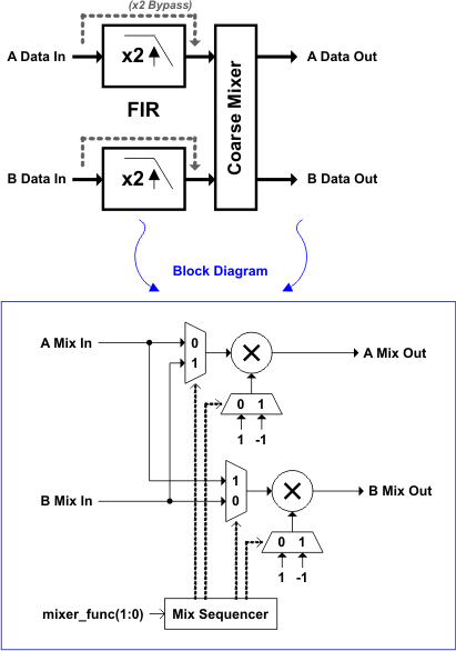 Figure 41. Coarse Mixers Block Diagram
The coarse mixer in the DAC3283 treats the A and B inputs as complex input data and for most mixing frequencies produces a complex output. Only when the mixing frequency is set to fS/2 the A and B channels can be maintained isolated as shown in Table 5. In this case, the two channels are upconverted as independent signals. By setting the mixer to fS/2 the interpolation filter outputs are inverted thus behaving as a high-pass filter.
Table 6. Dual-Channel Real Upconversion Options
| FIR MODE | INPUT FREQUENCY(1) | OUTPUT FREQUENCY(1) | SIGNAL BANDWIDTH(1) | SPECTRUM INVERTED? |
|---|---|---|---|---|
| Low Pass | 0.0 to 0.4 × fDATA | 0.0 to 0.4 × fDATA | 0.4 × fDATA | No |
| High Pass | 0.0 to 0.4 × fDATA | 0.6 to 1.0 × fDATA | 0.4 × fDATA | Yes |
8.4.11 Quadrature Modulation Correction (QMC)
The Quadrature Modulator Correction (QMC) block provides a means for adjusting the gain and phase of the complex signal. At a quadrature modulator output, gain and phase imbalances result in an undesired sideband signal.
The block diagram for the QMC is shown in Figure 42. The QMC block contains 3 programmable parameters: qmc_gaina(10:0), qmc_gainb(10:0) and qmc_phase(9:0).
Registers qmc_gaina(10:0) and qmc_gainb(10:0) control the I and Q path gains and are 11 bit values with a range of 0 to approximately 2. This value is used to scale the signal range. Register qmc_phase(9:0) controls the phase imbalance between I and Q and is a 10-bit value that ranges from –1/8 to approximately +1/8. This value is multiplied by each Q sample then summed into the I sample path. This operation is a simplified approximation of a true phase rotation and covers the range from –7.125 to +7.125 degrees in 1024 steps.
A write to register CONFIG27 is required to load the gain and phase values (CONFIG27-CONFIG30) into the QMC block simultaneously. When updating the gain and/or phase values CONFIG27 should be written last. Programming any of the other three registers will not affect the gain and phase settings.
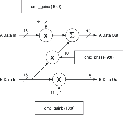 Figure 42. QMC Block Diagram
8.4.12 Digital Offset Control
The qmc_offseta(12:0) and qmc_offsetb(12:0) values in registers CONFIG20 through CONFIG23 can be used to independently adjust the A and B path DC offsets. Both offset values are in represented in 2s-complement format with a range from –4096 to 4095.
Note that a write to register CONFIG20 is required to load the values of all four qmc_offset registers (CONFIG20-CONFIG23) into the offset block simultaneously. When updating the offset values CONFIG20 should be written last. Programming any of the other three registers will not affect the offset setting.
The offset value adds a digital offset to the digital data before digital-to-analog conversion. Since the offset is added directly to the data it may be necessary to back off the signal to prevent saturation. Both data and offset values are LSB aligned.
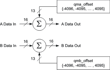 Figure 43. Digital Offset Block Diagram
8.4.13 Temperature Sensor
The DAC3283 incorporates a temperature sensor block which monitors the temperature by measuring the voltage across 2 transistors. The voltage is converted to an 8-bit digital word using a successive-approximation (SAR) analog to digital conversion process. The result is scaled, limited and formatted as a twos complement value representing the temperature in degrees Celsius.
The sampling is controlled by the serial interface signals SDENB and SCLK. If the temperature sensor is enabled (tsense_ena = 1 in register CONFIG24) a conversion takes place each time the serial port is written or read. The data is only read and sent out by the digital block when the temperature sensor is read in register CONFIG5. The conversion uses the first eight clocks of the serial clock as the capture and conversion clock, the data is valid on the falling eighth SCLK. The data is then clocked out of the chip on the rising edge of the ninth SCLK. No other clocks to the chip are necessary for the temperature sensor operation. As a result the temperature sensor is enabled even when the device is in sleep mode.
In order for the process described above to operate properly, the serial port read from CONFIG5 must be done with an SCLK period of at least 1µs. If this is not satisfied the temperature sensor accuracy is greatly reduced.
8.4.14 Sleep Modes
The DAC3283 features independent sleep control of each DAC (sleepa and sleepb), their corresponding clock path (clkpath_sleep_a and clkpath_sleep_b) as well as the clock input receiver of the device (clkrecv_sleep). The sleep control of each of these components is done through the SIF interface and is enabled by setting a 1 to the corresponding sleep register.
Complete power down of the device is set by setting all of these components to sleep. Under this mode the supply power consumption is reduced to 15mW. Power-up time in this case will be in the milliseconds range. Alternatively for those applications were power-up and power-down times are critical it is recommended to only set the DACs to sleep through the sleepa and sleepb registers. In this case both the sleep and wake-up times are only 90µs.
8.4.15 LVPECL Inputs
Figure 44 shows an equivalent circuit for the DAC input clock (DACCLP/N) and the output strobe clock (OSTRP/N).
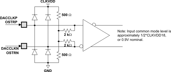 Figure 44. DACCLKP/N and OSTRP/N Equivalent Input Circuit
Figure 45 shows the preferred configuration for driving the CLKIN/CLKINC input clock with a differential ECL/PECL source.
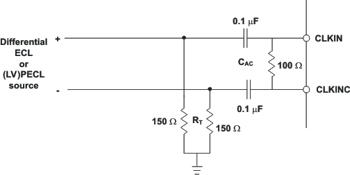 Figure 45. Preferred Clock Input Configuration with a Differential ECL/PECL Clock Source
8.4.16 LVDS INPUTS
The D[7:0]P/N, DATACLKP/N and FRAMEP/N LVDS pairs have the input configuration shown in Figure 46. Figure 47 shows the typical input levels and common-move voltage used to drive these inputs.
![DAC3283 D[7:0]P/N, DATACLKP/N
and FRAMEP/N LVDS Input Configuration DAC3283 LVDS_input_las693.gif](/ods/images/SLAS693C/LVDS_input_las693.gif) Figure 46. D[7:0]P/N, DATACLKP/N and FRAMEP/N LVDS Input Configuration
Figure 46. D[7:0]P/N, DATACLKP/N and FRAMEP/N LVDS Input Configuration
![DAC3283 LVDS Data (D[7:0]P/N,
DATACLKP/N, FRAMEP/N Pairs) Input Levels DAC3283 LVDS_data_las693.gif](/ods/images/SLAS693C/LVDS_data_las693.gif) Figure 47. LVDS Data (D[7:0]P/N, DATACLKP/N, FRAMEP/N Pairs) Input Levels
Figure 47. LVDS Data (D[7:0]P/N, DATACLKP/N, FRAMEP/N Pairs) Input Levels
Table 7. Example LVDS Data Input Levels
| APPLIED VOLTAGES | RESULTING DEFERENTIAL VOLTAGE | RESULTING COMMON-MODE VOLTAGE | LOGICAL BIT BINARY EQUIVALENT | |
|---|---|---|---|---|
| VA | VB | VA,B | VCOM | |
| 1.4 V | 1.0 V | 400 mV | 1.2 V | 1 |
| 1.0 V | 1.4 V | –400 mV | 0 | |
| 1.2 V | 0.8 V | 400 mV | 1.0 V | 1 |
| 0.8 V | 1.2 V | –400 mV | 0 | |
8.4.17 CMOS Digital Inputs
Figure 48 shows a schematic of the equivalent CMOS digital inputs of the DAC3283. SDIO, SCLK and TXENABLE have pull-down resistors while SDENB has a pull-up resistors internal to the DAC3283. See the specification table for logic thresholds. The pull-up and pull-down circuitry is approximately equivalent to 100kΩ.
 Figure 48. CMOS/TTL Digital Equivalent Input
8.4.18 Reference Operation
The DAC3283 uses a bandgap reference and control amplifier for biasing the full-scale output current. The full-scale output current is set by applying an external resistor RBIAS to pin BIASJ. The bias current IBIAS through resistor RBIAS is defined by the on-chip bandgap reference voltage and control amplifier. The default full-scale output current equals 16 times this bias current and can thus be expressed as:
IOUTFS = 16 × IBIAS = 16 × VEXTIO / RBIAS
Each DAC has a 4-bit coarse gain control via coarse_daca(3:0) and coarse_dacb (3:0) in the CONFIG4 register. Using gain control, the IOUTFS can be expressed as::
IOUTAFS = (DACA_gain + 1) × IBIAS = (DACA_gain + 1) × VEXTIO / RBIAS
IOUTBFS = (DACB_gain + 1) x IBIAS = (DACB_gain + 1) x VEXTIO / RBIAS
where VEXTIO is the voltage at terminal EXTIO. The bandgap reference voltage delivers an accurate voltage of 1.2V. This reference is active when extref_ena = '0' in CONFIG25. An external decoupling capacitor CEXT of 0.1µF should be connected externally to terminal EXTIO for compensation. The bandgap reference can additionally be used for external reference operation. In that case, an external buffer with high impedance input should be applied in order to limit the bandgap load current to a maximum of 100nA. The internal reference can be disabled and overridden by an external reference by setting the CONFIG25 extref_ena control bit. Capacitor CEXT may hence be omitted. Terminal EXTIO thus serves as either input or output node.
The full-scale output current can be adjusted from 20mA down to 2mA by varying resistor RBIAS or changing the externally applied reference voltage. The internal control amplifier has a wide input range, supporting the full-scale output current range of 20dB.
8.4.19 DAC Transfer Function
The CMOS DAC’s consist of a segmented array of NMOS current sinks, capable of sinking a full-scale output current up to 20mA. Differential current switches direct the current to either one of the complementary output nodes IOUT1 or IOUT2. (DACA = IOUTA1 or IOUTA2 and DACB = IOUTB1 or IOUTB2.) Complementary output currents enable differential operation, thus canceling out common mode noise sources (digital feed-through, on-chip and PCB noise), dc offsets, even order distortion components, and increasing signal output power by a factor of two.
The full-scale output current is set using external resistor RBIAS in combination with an on-chip bandgap voltage reference source (+1.2V) and control amplifier. Current IBIAS through resistor RBIAS is mirrored internally to provide a maximum full-scale output current equal to 16 times IBIAS.
The relation between IOUT1 and IOUT2 can be expressed as:
IOUT1 = – IOUTFS – IOUT2
Current flowing into a node is denoted as – current and current flowing out of a node as + current. Since the output stage is a current sink the current can only flow from AVDD into the IOUT1 and IOUT2 pins. The output current flow in each pin driving a resistive load can be expressed as:
IOUT1 = IOUTFS × (65535 – CODE) / 65536
IOUT2 = IOUTFS × CODE / 65536
where CODE is the decimal representation of the DAC data input word.
For the case where IOUT1 and IOUT2 drive resistor loads RL directly, this translates into single ended voltages at IOUT1 and IOUT2:
VOUT1 = AVDD – | IOUT1 | × RL
VOUT2 = AVDD – | IOUT2 | × RL
Assuming that the data is full scale (65536 in offset binary notation) and the RL is 25 Ω, the differential voltage between pins IOUT1 and IOUT2 can be expressed as:
VOUT1 = AVDD – | –0 mA | × 25 Ω = 3.3 V
VOUT2 = AVDD – | –20 mA | × 25 Ω = 2.8 V
VDIFF = VOUT1 – VOUT2 = 0.5 V
Note that care should be taken not to exceed the compliance voltages at node IOUT1 and IOUT2, which would lead to increased signal distortion.
8.4.20 Analog Current Outputs
Figure 49 shows a simplified schematic of the current source array output with corresponding switches. Differential switches direct the current of each individual NMOS current source to either the positive output node IOUT1 or its complementary negative output node IOUT2. The output impedance is determined by the stack of the current sources and differential switches, and is typically >300 kΩ in parallel with an output capacitance of 5 pF.
The external output resistors are referenced to an external ground. The minimum output compliance at nodes IOUT1 and IOUT2 is limited to AVDD – 0.5 V, determined by the CMOS process. Beyond this value, transistor breakdown may occur resulting in reduced reliability of the DAC3283 device. The maximum output compliance voltage at nodes IOUT1 and IOUT2 equals AVDD + 0.5 V. Exceeding the minimum output compliance voltage adversely affects distortion performance and integral non-linearity. The optimum distortion performance for a single-ended or differential output is achieved when the maximum full-scale signal at IOUT1 and IOUT2 does not exceed 0.5 V.
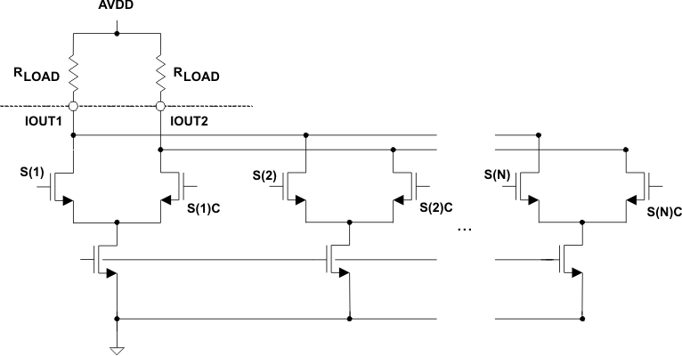 Figure 49. Equivalent Analog Current Output
The DAC3283 can be easily configured to drive a doubly terminated 50Ω cable using a properly selected RF transformer. Figure 50 and Figure 51 show the 50Ω doubly terminated transformer configuration with 1:1 and 4:1 impedance ratio, respectively. Note that the center tap of the primary input of the transformer has to be connected to AVDD to enable a dc current flow. Applying a 20 mA full-scale output current would lead to a 0.5 VPP for a 1:1 transformer, and a 1 VPP output for a 4:1 transformer. The low dc-impedance between IOUT1 or IOUT2 and the transformer center tap sets the center of the ac-signal at AVDD, so the 1 VPP output for the 4:1 transformer results in an output between AVDD + 0.5 V and AVDD – 0.5 V.
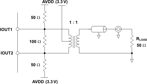 Figure 50. Driving a Doubly-Terminated 50-Ω Cable Using a 1:1 Impedance Ratio Transformer
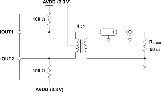 Figure 51. Driving a Doubly-Terminated 50-Ω Cable Using a 4:1 Impedance Ratio Transformer
8.4.21 Passive Interface to Analog Quadrature Modulators
A common application in communication systems is to interface the DAC to an IQ modulator like the TRF3703 family of modulators from Texas Instruments. The input of the modulator is generally of high impedance and requires a specific common-mode voltage. A simple resistive network can be used to maintain 50Ω load impedance for the DAC3283 and also provide the necessary common-mode voltages for both the DAC and the modulator.
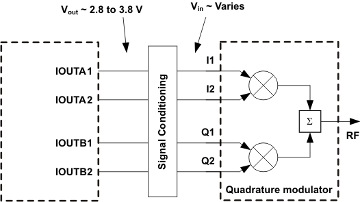 Figure 52. DAC to Analog Quadrature Modulator Interface
The DAC3283 has a maximum 20mA full-scale output and a voltage compliance range of AVDD ± 0.5 V. The TRF3703 IQ modulator family can be operated at three common-mode voltages: 1.5V, 1.7V, and 3.3V.
Figure 53 shows the recommended passive network to interface the DAC3283 to the TRF3703-17 which has a common mode voltage of 1.7V. The network generates the 3.3V common mode required by the DAC output and 1.7V at the modulator input, while still maintaining 50Ω load for the DAC.
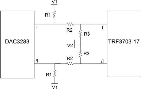 Figure 53. DAC3283 to TRF3703-17 Interface
If V1 is set to 5V and V2 is set to -5V, the corresponding resistor values are R1 = 57Ω, R2 = 80Ω, and
R3 = 336Ω. The loss developed through R2 is about –1.86 dB. In the case where there is no –5V supply available and V2 is set to 0V, the resistor values are R1 = 66Ω, R2 = 101Ω, and R3 = 107Ω. The loss with these values is –5.76dB.
Figure 54 shows the recommended network for interfacing with the TRF3703-33 which requires a common mode of 3.3V. This is the simplest interface as there is no voltage shift. Because there is no voltage shift there is any loss in the network. With V1 = 5V and V2 = 0V, the resistor values are R1 = 66Ω and R3 = 208Ω.
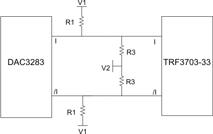 Figure 54. DAC3283 to TRF3703-33 Interface
In most applications, a baseband filter is required between the DAC and the modulator to eliminate the DAC images. This filter can be placed after the common-mode biasing network. For the DAC to modulator network shown in Figure 55, R2 and the filter load R4 need to be considered into the DAC impedance. The filter has to be designed for the source impedance created by the resistor combination of R3 // (R2+R1). The effective impedance seen by the DAC is affected by the filter termination resistor resulting in R1 // (R2+R3 // (R4/2)).
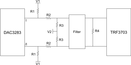 Figure 55. DAC3283 to Modulator Interface with Filter
Factoring in R4 into the DAC load, a typical interface to the TRF3703-17 with V1 = 5V and V2 = 0V results in the following values: R1 = 72Ω, R2 = 116Ω, R3 = 124Ω and R4 = 150Ω. This implies that the filter needs to be designed for 75Ω input and output impedance (single-ended impedance). The common mode levels for the DAC and modulator are maintained at 3.3V and 1.7V and the DAC load is 50Ω. The added load of the filter termination causes the signal to be attenuated by –10.8 dB.
A filter can be implemented in a similar manner to interface with the TRF3703-33. In this case it is much simpler to balance the loads and common mode voltages due to the absence of R2. An added benefit is that there is no loss in this network. With V1 = 5V and V2 = 0V the network can be designed such that R1 = 115Ω, R3 = 681Ω, and R4 = 200Ω. This results in a filter impedance of R1 // R2=100Ω, and a DAC load of R1 // R3 // (R4/2) which is equal to 50Ω. R4 is a differential resistor and does not affect the common mode level created by R1 and R3. The common-mode voltage is set at 3.3 V for a full-scale current of 20mA.
For more information on how to interface the DAC3283 to an analog quadrature modulator please refer to the application reports Passive Terminations for Current Output DACs (SLAA399) and Design of Differential Filters for High-Speed Signal Chains (SLWA053).
8.5 Register Maps
Table 8. Register Map
8.5.1 CONFIG0 (address = 0x00) [reset = 0x70]
| 7 | 6 | 5 | 4 | 3 | 2 | 1 | 0 |
| Reserved | fifo_ena | fifo_reset_ena | multi_sync_ena | alarm_out_ena | alarm_pol | mixer_func(1:0) | |
| R/W | R/W | R/W | R/W | R/W | R/W | R/W | R/W |
| LEGEND: R/W = Read/Write; R = Read only; -n = value after reset |
Table 9. CONFIG0 Field Descriptions
8.5.2 CONFIG1 (address = 0x01) [reset = 0x11]
| 7 | 6 | 5 | 4 | 3 | 2 | 1 | 0 |
| qmc_offset_ena | qmc_correct_ena | fir0_ena | fir1_ena | Unused | iotest_ena | Unused | twos |
| R/W | R/W | R/W | R/W | R/W | R/W | R/W | R/W |
| LEGEND: R/W = Read/Write; R = Read only; -n = value after reset |
Table 10. CONFIG1 Field Descriptions
| Bit | Field | Type | Reset | Description |
|---|---|---|---|---|
| 7 | qmc_offset_ena | R/W | 0 | When asserted the QMC offset correction circuitry is enabled. |
| 6 | qmc_correct_ena | R/W | 0 | When asserted the QMC phase and gain correction circuitry is enabled. |
| 5 | fir0_ena | R/W | 0 | When asserted FIR0 is activated enabling 2x interpolation. |
| 4 | fir1_ena | R/W | 1 | When asserted FIR1 is activated enabling 4x interpolation. fir0_ena must be set to '1' for 4x interpolation. |
| 3 | Unused | R/W | 0 | Reserved for factory use. |
| 2 | iotest_ena | R/W | 0 | When asserted enables the data pattern checker operation. |
| 1 | Unused | R/W | 0 | Reserved for factory use. |
| 0 | twos | R/W | 1 | When asserted the inputs are expected to be in 2's complement format. When de-asserted the input format is expected to be offset-binary. |
8.5.3 CONFIG2 (address = 0x02) [reset = 0x00]
| 7 | 6 | 5 | 4 | 3 | 2 | 1 | 0 |
| Unused | Unused | sif_sync | sif_sync_ena | Unused | Unused | out_delay | |
| R/W | R/W | R/W | R/W | R/W | R/W | R/W | R/W |
| LEGEND: R/W = Read/Write; R = Read only; -n = value after reset |
Table 11. CONFIG2 Field Descriptions
8.5.4 CONFIG3 (address = 0x03) [reset = 0x10]
| 7 | 6 | 5 | 4 | 3 | 2 | 1 | 0 |
| 64cnt_ena | Unused | Unused | fifo_offset(2:0) | alarm_2away_ena | alarm_1away_ena | ||
| R/W | R/W | R/W | R/W | R/W | R/W | R/W | R/W |
| LEGEND: R/W = Read/Write; R = Read only; -n = value after reset |
Table 12. CONFIG3 Field Descriptions
| Bit | Field | Type | Reset | Description |
|---|---|---|---|---|
| 7 | 64cnt_ena | R/W | 0 | This enables resetting the alarms after 64 good samples with the goal of removing unnecessary errors. For instance, when checking setup/hold through the pattern checker test, there may initially be errors. Setting this bit removes the need for a SIF write to clear the alarm register. |
| 6 | Unused | R/W | 0 | Reserved for factory use. |
| 5 | Unused | R/W | 0 | Reserved for factory use. |
| 4:2 | fifo_offset(2:0) | R/W | 100 | This is the default FIFO read pointer position after the FIFO read pointer has been synced. With this value the initial difference between write and read pointers can be controlled. This may be helpful in controlling the delay through the device. |
| 1 | alarm_2away_ena | R/W | 0 | When asserted alarms from the FIFO that represent the write and read pointers being 2 away are enabled. |
| 0 | alarm_1away_ena | R/W | 0 | When asserted alarms from the FIFO that represent the write and read pointers being 1 away are enabled. |
8.5.5 CONFIG4 (address = 0x04) [reset = 0xFF]
| 7 | 6 | 5 | 4 | 3 | 2 | 1 | 0 |
| coarse_daca(3:0) | coarse_dach(3:0) | ||||||
| R/W | R/W | R/W | R/W | R/W | R/W | R/W | R/W |
| LEGEND: R/W = Read/Write; R = Read only; -n = value after reset |
Table 13. CONFIG4 Field Descriptions
| Bit | Field | Type | Reset | Description |
|---|---|---|---|---|
| 7:4 | coarse_daca(3:0) | R/W | 1111 | Scales the DACA output current in 16 equal steps. |
 |
||||
| 3:0 | coarse_dach(3:0) | R/W | 1111 | Scales the DACB output current in 16 equal steps. |
8.5.6 CONFIG5 (address = 0x05) READ ONLY
| 7 | 6 | 5 | 4 | 3 | 2 | 1 | 0 |
| tempdata | |||||||
| R | R | R | R | R | R | R | R |
| LEGEND: R/W = Read/Write; R = Read only; -n = value after reset |
Table 14. CONFIG5 Field Descriptions
| Bit | Field | Type | Reset | Description |
|---|---|---|---|---|
| 7:0 | tempdata | R | N/A | This is the output from the chip temperature sensor. The value of this register in two’s complement format represents the temperature in degrees Celsius. This register must be read with a minimum SCLK period of 1µs. (Read Only) |
8.5.7 CONFIG6 (address =0x06) [reset = 0x00]
| 7 | 6 | 5 | 4 | 3 | 2 | 1 | 0 |
| Unused | alarm_mask | ||||||
| R/W | R/W | R/W | R/W | R/W | R/W | R/W | R/W |
| LEGEND: R/W = Read/Write; R = Read only; -n = value after reset |
Table 15. CONFIG6 Field Descriptions
| Bit | Field | Type | Reset | Description | |
|---|---|---|---|---|---|
| 7 | Unused | R/W | 0 | Reserved for factory use. | |
| 6:0 | alarm_mask | R/W | 0000000 | These bits control the masking of the alarm outputs. This means that the ALARM_SDO pin will not be asserted if the appropriate bit is set. The alarm will still show up in the CONFIG7 bits. (0=not masked, 1= masked). | |
| alarm_mask | Masked Alarm | ||||
| 6 | alarm_from_zerochk | ||||
| 5 | alarm_fifo_collision | ||||
| 4 | reserved | ||||
| 3 | alarm_from_iotest | ||||
| 2 | not used (expansion) | ||||
| 1 | alarm_fifo_2away | ||||
| 0 | alarm_fifo_1away | ||||
8.5.8 CONFIG7 (address = 0x07) [reset = 0x00] (WRITE TO CLEAR)
| 7 | 6 | 5 | 4 | 3 | 2 | 1 | 0 |
| Unused | alarm_from_ zerochk |
alarm_fifo_ collision |
Reserved | alarm_from_ iotest |
Unused | alarm_fifo_ 2away |
alarm_fifo_ 1away |
| W | W | W | W | W | W | W | W |
| LEGEND: R/W = Read/Write; R = Read only; -n = value after reset |
Table 16. CONFIG7 Field Descriptions
8.5.9 CONFIG8 (address = 0x08) [reset = 0x00] (WRITE TO CLEAR)
| 7 | 6 | 5 | 4 | 3 | 2 | 1 | 0 |
| iotest_results | |||||||
| R/W | R/W | R/W | R/W | R/W | R/W | R/W | R/W |
| LEGEND: R/W = Read/Write; R = Read only; -n = value after reset |
8.5.10 CONFIG9 (address = 0x09) [reset = 0x7A]
| 7 | 6 | 5 | 4 | 3 | 2 | 1 | 0 |
| iotest_pattern0 | |||||||
| R/W | R/W | R/W | R/W | R/W | R/W | R/W | R/W |
| LEGEND: R/W = Read/Write; R = Read only; -n = value after reset |
Table 18. CONFIG9 Field Descriptions
| Bit | Field | Type | Reset | Description |
|---|---|---|---|---|
| 7:0 | iotest_pattern0 | R/W | 0x7A | This is dataword0 in the IO test pattern. It is used with the seven other words to test the input data. |
8.5.11 CONFIG10 (address = 0x0A) [reset = 0xB6]
| 7 | 6 | 5 | 4 | 3 | 2 | 1 | 0 |
| iotest_pattern1 | |||||||
| R/W | R/W | R/W | R/W | R/W | R/W | R/W | R/W |
| LEGEND: R/W = Read/Write; R = Read only; -n = value after reset |
Table 19. CONFIG10 Field Descriptions
| Bit | Field | Type | Reset | Description |
|---|---|---|---|---|
| 7:0 | iotest_pattern1 | R/W | 0xB6 | This is dataword1 in the IO test pattern. It is used with the seven other words to test the input data. |
8.5.12 CONFIG11 (address = 0x0B) [reset = 0xEA]
| 7 | 6 | 5 | 4 | 3 | 2 | 1 | 0 |
| iotest_pattern2 | |||||||
| R/W | R/W | R/W | R/W | R/W | R/W | R/W | R/W |
| LEGEND: R/W = Read/Write; R = Read only; -n = value after reset |
Table 20. CONFIG11 Field Descriptions
| Bit | Field | Type | Reset | Description |
|---|---|---|---|---|
| 7:0 | iotest_pattern2 | R/W | 0xB6 | This is dataword2 in the IO test pattern. It is used with the seven other words to test the input data. |
8.5.13 CONFIG12 (address =0x0C) [reset = 0x45]
| 7 | 6 | 5 | 4 | 3 | 2 | 1 | 0 |
| iotest_pattern3 | |||||||
| R/W | R/W | R/W | R/W | R/W | R/W | R/W | R/W |
| LEGEND: R/W = Read/Write; R = Read only; -n = value after reset |
Table 21. CONFIG12 Field Descriptions
| Bit | Field | Type | Reset | Description |
|---|---|---|---|---|
| 7:0 | iotest_pattern3 | R/W | 0x45 | This is dataword3 in the IO test pattern. It is used with the seven other words to test the input data. |
8.5.14 CONFIG13 (address =0x0D) [reset = 0x1A]
| 7 | 6 | 5 | 4 | 3 | 2 | 1 | 0 |
| iotest_pattern4 | |||||||
| R/W | R/W | R/W | R/W | R/W | R/W | R/W | R/W |
| LEGEND: R/W = Read/Write; R = Read only; -n = value after reset |
Table 22. CONFIG13 Field Descriptions
| Bit | Field | Type | Reset | Description |
|---|---|---|---|---|
| 7:0 | iotest_pattern4 | R/W | 0x1A | This is dataword4 in the IO test pattern. It is used with the seven other words to test the input data. |
8.5.15 CONFIG14 Register Name (address = 0x0E) [reset = 0x16]
| 7 | 6 | 5 | 4 | 3 | 2 | 1 | 0 |
| iotest_pattern5 | |||||||
| R/W | R/W | R/W | R/W | R/W | R/W | R/W | R/W |
| LEGEND: R/W = Read/Write; R = Read only; -n = value after reset |
Table 23. CONFIG14 Field Descriptions
| Bit | Field | Type | Reset | Description |
|---|---|---|---|---|
| 7:0 | iotest_pattern5 | R/W | 0x16 | This is dataword5 in the IO test pattern. It is used with the seven other words to test the input data. |
8.5.16 CONFIG15 Register Name (address = 0x0F) [reset = 0xAA]
| 7 | 6 | 5 | 4 | 3 | 2 | 1 | 0 |
| iotest_pattern6 | |||||||
| R/W | R/W | R/W | R/W | R/W | R/W | R/W | R/W |
| LEGEND: R/W = Read/Write; R = Read only; -n = value after reset |
Table 24. CONFIG15 Field Descriptions
| Bit | Field | Type | Reset | Description |
|---|---|---|---|---|
| 7:0 | iotest_pattern6 | R/W | 0xAA | This is dataword6 in the IO test pattern. It is used with the seven other words to test the input data. |
8.5.17 CONFIG16 (address = 0x10) [reset = 0xV6]
| 7 | 6 | 5 | 4 | 3 | 2 | 1 | 0 |
| iotest_pattern7 | |||||||
| R/W | R/W | R/W | R/W | R/W | R/W | R/W | R/W |
| LEGEND: R/W = Read/Write; R = Read only; -n = value after reset |
Table 25. CONFIG16 Field Descriptions
| Bit | Field | Type | Reset | Description |
|---|---|---|---|---|
| 7:0 | iotest_pattern7 | R/W | 0xC6 | This is dataword7 in the IO test pattern. It is used with the seven other words to test the input data. |
8.5.18 CONFIG17 (address = 0x11) [reset = 0x24]
| 7 | 6 | 5 | 4 | 3 | 2 | 1 | 0 |
| Reserved | Reserved | Reserved | clk_alarm_mask | tx_off_mask | Reserved | clk_alarm_ena | tx_off_ena |
| R/W | R/W | R/W | R/W | R/W | R/W | R/W | R/W |
| LEGEND: R/W = Read/Write; R = Read only; -n = value after reset |
Table 26. CONFIG17 Field Descriptions
| Bit | Field | Type | Reset | Description |
|---|---|---|---|---|
| 7 | Reserved | R/W | 0 | Reserved for factory use. |
| 6 | Reserved | R/W | 0 | Reserved for factory use. |
| 5 | Reserved | R/W | 1 | Reserved for factory use. |
| 4 | clk_alarm_mask | R/W | 0 | This bit controls the masking of the clock monitor alarm. This means that the ALARM_SDO pin will not be asserted. The alarm will still show up in the clk_alarm bit. (0=not masked, 1= masked). |
| 3 | tx_off_mask | R/W | 0 | This bit control the masking of the transmit enable alarm. This means that the ALARM_SDO pin will not be asserted. The alarm will still show up in the tx_off bit. (0=not masked, 1= masked). |
| 2 | Reserved | R/W | 1 | Reserved for factory use. |
| 1 | clk_alarm_ena | R/W | 0 | When asserted the DATACLK monitor alarm is enabled. |
| 0 | tx_off_ena | R/W | 0 | When asserted a clk_alarm event will automatically disable the DAC outputs by setting them to midscale. |
8.5.19 CONFIG18 (address = 0x12) [reset = 0x02]
| 7 | 6 | 5 | 4 | 3 | 2 | 1 | 0 |
| Reserved | daca_complement | dacb_complement | clkdiv_sync_ena | Unused | |||
| R/W | R/W | R/W | R/W | R/W | R/W | R/W | R/W |
| LEGEND: R/W = Read/Write; R = Read only; -n = value after reset |
Table 27. CONFIG18 Field Descriptions
8.5.20 CONFIG19 (address = 0x13) [reset = 0x00]
| 7 | 6 | 5 | 4 | 3 | 2 | 1 | 0 |
| bequalsa | aequalsb | Reserved | Unused | Unused | Unused | multi_sync_sel | rev |
| R/W | R/W | R/W | R/W | R/W | R/W | R/W | R/W |
| LEGEND: R/W = Read/Write; R = Read only; -n = value after reset |
Table 28. CONFIG19 Field Descriptions
| Bit | Field | Type | Reset | Description | |
|---|---|---|---|---|---|
| 7 | bequalsa | R/W | 0 | When asserted the DACA data is driven onto DACB. | |
| 6 | aequalsb | R/W | 0 | When asserted the DACB data is driven onto DACA. | |
| 5 | Reserved | R/W | 0 | Reserved for factory use. | |
| 4 | Unused | R/W | 0 | Reserved for factory use. | |
| 3 | Unused | R/W | 0 | Reserved for factory use. | |
| 2 | Unused | R/W | 0 | Reserved for factory use. | |
| 1 | multi_sync_sel | R/W | 0 | Selects the signal source for multiple device and clock divider synchronization. | |
| multi_sync_sel | Sync Source | ||||
| 0 | OSTR | ||||
| 1 | FRAME through FIFO handoff | ||||
| 0 | rev | R/W | 0 | Reverse the input bits for the data word. MSB becomes LSB. | |
8.5.21 CONFIG20 (address = 0x14) [reset = 0x00] (CAUSES AUTOSYNC)
| 7 | 6 | 5 | 4 | 3 | 2 | 1 | 0 |
| qmc_offseta | |||||||
| R/W | R/W | R/W | R/W | R/W | R/W | R/W | R/W |
| LEGEND: R/W = Read/Write; R = Read only; -n = value after reset |
Table 29. CONFIG20 Field Descriptions
| Bit | Field | Type | Reset | Description |
|---|---|---|---|---|
| 7:0 | qmc_offseta | R/W | 0x00 | Lower 8 bits of the DAC A offset correction. The offset is measured in DAC LSBs. Writing this register causes an autosync to be generated. This loads the values of all four qmc_offset registers (CONFIG20-CONFIG23) into the offset block at the same time. When updating the offset values CONFIG20 should be written last. Programming any of the other three registers will not affect the offset setting. |
8.5.22 CONFIG21 (address = 0x15) [reset = 0x00]
| 7 | 6 | 5 | 4 | 3 | 2 | 1 | 0 |
| qmc_offsetb | |||||||
| R/W | R/W | R/W | R/W | R/W | R/W | R/W | R/W |
| LEGEND: R/W = Read/Write; R = Read only; -n = value after reset |
Table 30. CONFIG21 Field Descriptions
| Bit | Field | Type | Reset | Description |
|---|---|---|---|---|
| 7:0 | qmc_offsetb | R/W | 0x00 | Lower 8 bits of the DAC B offset correction. The offset is measured in DAC LSBs. |
8.5.23 CONFIG22 (address = 0x16) [reset = 0x00]
| 7 | 6 | 5 | 4 | 3 | 2 | 1 | 0 |
| qmc_offseta | Unused | Unused | Unused | ||||
| R/W | R/W | R/W | R/W | R/W | R/W | R/W | R/W |
| LEGEND: R/W = Read/Write; R = Read only; -n = value after reset |
Table 31. CONFIG22 Field Descriptions
| Bit | Field | Type | Reset | Description |
|---|---|---|---|---|
| 7:3 | qmc_offseta | R/W | 00000 | Upper 5 bits of the DAC A offset correction. |
| 2 | Unused | R/W | 0 | Reserved for factory use. |
| 1 | Unused | R/W | 0 | Reserved for factory use. |
| 0 | Unused | R/W | 0 | Reserved for factory use. |
8.5.24 CONFIG23 (address = 0x17) [reset = 0x00]
| 7 | 6 | 5 | 4 | 3 | 2 | 1 | 0 |
| qmc_offsetb(12:8) | sif4_ena | clkpath_sleep_a | clkpath_sleep_b | ||||
| R/W | R/W | R/W | R/W | R/W | R/W | R/W | R/W |
| LEGEND: R/W = Read/Write; R = Read only; -n = value after reset |
Table 32. CONFIG23 Field Descriptions
| Bit | Field | Type | Reset | Description |
|---|---|---|---|---|
| 7:3 | qmc_offsetb(12:8) | R/W | 00000 | Upper 5 bits of the DAC B offset correction. |
| 2 | sif4_ena | R/W | 0 | When asserted the SIF interface becomes a 4 pin interface. The ALARM pin is turned into a dedicated output for the reading of data. |
| 1 | clkpath_sleep_a | R/W | 0 | When asserted puts the clock path through DAC A to sleep. This is useful for sleeping individual DACs. Even if the DAC is asleep the clock needs to pass through it for the logic to work. However, if the chip is being put into a power down mode, then all parts of the DAC can be turned off. |
| 0 | clkpath_sleep_b | R/W | 0 | When asserted puts the clock path through DAC B to sleep. |
8.5.25 CONFIG24 (address = 0x18) [reset = 0x83]
| 7 | 6 | 5 | 4 | 3 | 2 | 1 | 0 |
| tsense_ena | clkrecv_sleep | Unused | Reserved | sleepb | sleepa | Reserved | Reserved |
| R/W | R/W | R/W | R/W | R/W | R/W | R/W | R/W |
| LEGEND: R/W = Read/Write; R = Read only; -n = value after reset |
Table 33. CONFIG24 Field Descriptions
| Bit | Field | Type | Reset | Description |
|---|---|---|---|---|
| 7 | tsense_ena | R/W | 1 | Turns on the temperature sensor when asserted. |
| 6 | clkrecv_sleep | R/W | 0 | When asserted the clock input receiver gets put into sleep mode. This also affects the OSTR receiver. |
| 5 | Unused | R/W | 0 | Reserved for factory use. |
| 4 | Reserved | R/W | 0 | Reserved for factory use. |
| 3 | sleepb | R/W | 0 | When asserted DACB is put into sleep mode. |
| 2 | sleepa | R/W | 0 | When asserted DACA is put into sleep mode. |
| 1 | Reserved | R/W | 1 | Reserved for factory use. |
| 0 | Reserved | R/W | 1 | Reserved for factory use. |
8.5.26 CONFIG25 (address = 0x19) [reset = 0x00]
| 7 | 6 | 5 | 4 | 3 | 2 | 1 | 0 |
| Reserved | extref_ena | Reserved | Reserved | ||||
| R/W | R/W | R/W | R/W | R/W | R/W | R/W | R/W |
| LEGEND: R/W = Read/Write; R = Read only; -n = value after reset |
Table 34. CONFIG25 Field Descriptions
| Bit | Field | Type | Reset | Description |
|---|---|---|---|---|
| 7:3 | Reserved | R/W | 00000 | Turns on the temperature sensor when asserted. |
| 2 | extref_ena | R/W | 0 | Allows the device to use an external reference or the internal reference. (0=internal, 1=external) |
| 1 | Reserved | R/W | 0 | Reserved for factory use. |
| 0 | Reserved | R/W | 0 | Reserved for factory use. |
8.5.27 CONFIG26 (address = 0x1a) [reset = 0x00]
| 7 | 6 | 5 | 4 | 3 | 2 | 1 | 0 |
| Reserved | Reserved | Unused | Reserved | ||||
| R/W | R/W | R/W | R/W | R/W | R/W | R/W | R/W |
| LEGEND: R/W = Read/Write; R = Read only; -n = value after reset |
Table 35. CONFIG26 Field Descriptions
| Bit | Field | Type | Reset | Description |
|---|---|---|---|---|
| 7:6 | Reserved | R/W | 00 | Reserved for factory use. |
| 5:4 | Reserved | R/W | 00 | Reserved for factory use. |
| 3 | Unused | R/W | 0 | Reserved for factory use. |
| 2:0 | Reserved | R/W | 000 | Reserved for factory use. |
8.5.28 CONFIG27 (address =0x1b) [reset = 0x00] (CAUSES AUTOSYNC)
| 7 | 6 | 5 | 4 | 3 | 2 | 1 | 0 |
| qmc_gaina | |||||||
| R/W | R/W | R/W | R/W | R/W | R/W | R/W | R/W |
| LEGEND: R/W = Read/Write; R = Read only; -n = value after reset |
Table 36. CONFIG27 Field Descriptions
| Bit | Field | Type | Reset | Description |
|---|---|---|---|---|
| 7:0 | qmc_gaina | R/W | 0x00 | Lower 8 bits of the 11-bit DAC A QMC gain word. The upper 3 bits are located in the CONFIG30 register. The full 11-bit qmc_gaina(10:0) value is formatted as UNSIGNED with a range of 0 to 1.9990 and a default gain of 1. The implied decimal point for the multiplication is between bits 9 and 10. Writing this register causes an autosync to be generated. This loads the values of all four qmc_phase/gain registers (CONFIG27-CONFIG30) into the QMC block at the same time. When updating the QMC phase and/or gain values CONFIG27 should be written last. Programming any of the other three registers will not affect the QMC settings. |
8.5.29 CONFIG28 (address = 0x1C) [reset = 0x00]
| 7 | 6 | 5 | 4 | 3 | 2 | 1 | 0 |
| gmc_gainb | |||||||
| R/W | R/W | R/W | R/W | R/W | R/W | R/W | R/W |
| LEGEND: R/W = Read/Write; R = Read only; -n = value after reset |
Table 37. CONFIG28 Field Descriptions
| Bit | Field | Type | Reset | Description |
|---|---|---|---|---|
| 7:0 | gmc_gainb | R/W | 0x00 | Lower 8 bits of the 11-bit DAC B QMC gain word. The upper 3 bits are located in the CONFIG30 register. Refer to CONFIG27 for formatting. |
8.5.30 CONFIG29 (address = 0x1D) [reset = 0x00]
| 7 | 6 | 5 | 4 | 3 | 2 | 1 | 0 |
| qmc_phase | |||||||
| R/W | R/W | R/W | R/W | R/W | R/W | R/W | R/W |
| LEGEND: R/W = Read/Write; R = Read only; -n = value after reset |
Table 38. CONFIG29 Field Descriptions
| Bit | Field | Type | Reset | Description |
|---|---|---|---|---|
| 7:0 | qmc_phase | R/W | 0x00 | Lower 8-bits of the 10-bit QMC phase word. The upper 2 bits are in the CONFIG30 register. The full 10-bit qmc_phase(9:0) word is formatted as two's complement and scaled to occupy a range of –0.125 to 0.12475 (note this value does not correspond to degrees) and a default phase correction of 0. To accomplish QMC phase correction, this value is multiplied by the current 'Q' sample, then summed into the ‘I’ sample. |
8.5.31 CONFIG30 (address = 0x1E) [reset = 0x24]
| 7 | 6 | 5 | 4 | 3 | 2 | 1 | 0 |
| qmc_phase(9:8) | qmc_gaina(10:8) | qmc_gainb(10:8) | |||||
| R/W | R/W | R/W | R/W | R/W | R/W | R/W | R/W |
| LEGEND: R/W = Read/Write; R = Read only; -n = value after reset |
Table 39. CONFIG30 Field Descriptions
| Bit | Field | Type | Reset | Description |
|---|---|---|---|---|
| 7:6 | qmc_phase(9:8) | R/W | 00 | Upper 2 bits of qmc_phase. Defaults to zero. |
| 5:3 | qmc_gaina(10:8) | R/W | 100 | Upper 3 bits of qmc_gaina. Defaults to unity gain. |
| 2:0 | qmc_gainb(10:8) | R/W | 100 | Upper 3 bits of qmc_gainb. Defaults to unity gain. |
8.5.32 VERSION31 (address = 0x1F) [reset = 0x12] (PARTIAL READ ONLY)
| 7 | 6 | 5 | 4 | 3 | 2 | 1 | 0 |
| clk_alarm | tx_off | version(5:0) | |||||
| R | R | R | R | R | R | R | R |
| LEGEND: R/W = Read/Write; R = Read only; -n = value after reset |
Table 40. VERSION31 Field Descriptions
| Bit | Field | Type | Reset | Description |
|---|---|---|---|---|
| 7 | clk_alarm | R | 0 | This bit is set to '1' when DATACLK is stopped for 4 clock cycles. Once set, the bit needs to be cleared by writing a '0'. |
| 6 | tx_off | R | 0 | This bit is set to '1' when the clk_alarm is triggered. When set the DAC outputs are forced to mid-level. Once set, the bit needs to be cleared by writing a '0'. |
| 5:0 | version(5:0) | R | 010010 | A hardwired register that contains the version of the chip. (Read Only) |
