SLAS748G March 2011 – January 2024 DAC3482
PRODUCTION DATA
- 1
- 1 Features
- 2 Applications
- 3 Description
- 4 Pin Configuration and Functions
-
5 Specifications
- 5.1 Absolute Maximum Ratings
- 5.2 ESD Ratings
- 5.3 Recommended Operating Conditions
- 5.4 Thermal Information
- 5.5 Electrical Characteristics – DC Specifications
- 5.6 Electrical Characteristics – Digital Specifications
- 5.7 Electrical Characteristics – AC Specifications
- 5.8 Electrical Characteristics - Phase-Locked Loop Specifications
- 5.9 Timing Requirements - Digital Specifications
- 5.10 Switching Characteristics – AC Specifications
- 5.11 Typical Characteristics
-
6 Detailed Description
- 6.1 Overview
- 6.2 Functional Block Diagram
- 6.3
Feature Description
- 6.3.1 Serial Interface
- 6.3.2 Data Interface
- 6.3.3 Input FIFO
- 6.3.4 FIFO Modes of Operation
- 6.3.5 Clocking Modes
- 6.3.6 FIR Filters
- 6.3.7 Complex Signal Mixer
- 6.3.8 Quadrature Modulation Correction (QMC)
- 6.3.9 Temperature Sensor
- 6.3.10 Data Pattern Checker
- 6.3.11 Parity Check Test
- 6.3.12 DAC3482 Alarm Monitoring
- 6.3.13 LVPECL Inputs
- 6.3.14 LVDS Inputs
- 6.3.15 Unused LVDS Port Termination
- 6.3.16 CMOS Digital Inputs
- 6.3.17 Reference Operation
- 6.3.18 DAC Transfer Function
- 6.3.19 Analog Current Outputs
- 6.4 Device Functional Modes
- 6.5 Programming
- 6.6
Register Map
- 6.6.1
Register Descriptions
- 6.6.1.1 Register Name: config0 – Address: 0x00, Default: 0x049C
- 6.6.1.2 Register Name: config1 – Address: 0x01, Default: 0x050E
- 6.6.1.3 Register Name: config2 – Address: 0x02, Default: 0x7000
- 6.6.1.4 Register Name: config3 – Address: 0x03, Default: 0xF000
- 6.6.1.5 Register Name: config4 – Address: 0x04, Default: No RESET Value (WRITE TO CLEAR)
- 6.6.1.6 Register Name: config5 – Address: 0x05, Default: Setup and Power-Up Conditions Dependent (WRITE TO CLEAR)
- 6.6.1.7 Register Name: config6 – Address: 0x06, Default: No RESET Value (READ ONLY)
- 6.6.1.8 Register Name: config7 – Address: 0x07, Default: 0xFFFF
- 6.6.1.9 Register Name: config8 – Address: 0x08, Default: 0x0000 (CAUSES AUTO-SYNC)
- 6.6.1.10 Register Name: config9 – Address: 0x09, Default: 0x8000
- 6.6.1.11 Register Name: config10 – Address: 0x0A, Default: 0x0000
- 6.6.1.12 Register Name: config11 – Address: 0x0B, Default: 0x0000
- 6.6.1.13 Register Name: config12 – Address: 0x0C, Default: 0x0400
- 6.6.1.14 Register Name: config13 – Address: 0x0D, Default: 0x0400
- 6.6.1.15 Register Name: config14 – Address: 0x0E, Default: 0x0400
- 6.6.1.16 Register Name: config15 – Address: 0x0F, Default: 0x0400
- 6.6.1.17 Register Name: config16 – Address: 0x10, Default: 0x0000 (CAUSES AUTO-SYNC)
- 6.6.1.18 Register Name: config17 – Address: 0x11, Default: 0x0000
- 6.6.1.19 Register Name: config18 – Address: 0x12, Default: 0x0000 (CAUSES AUTO-SYNC)
- 6.6.1.20 Register Name: config19 – Address: 0x13, Default: 0x0000
- 6.6.1.21 Register Name: config20 – Address: 0x14, Default: 0x0000
- 6.6.1.22 Register Name: config21 – Address: 0x15, Default: 0x0000
- 6.6.1.23 Register name: config22 – Address: 0x16, Default: 0x0000
- 6.6.1.24 Register Name: config23 – Address: 0x17, Default: 0x0000
- 6.6.1.25 Register Name: config24 – Address: 0x18, Default: NA
- 6.6.1.26 Register Name: config25 – Address: 0x19, Default: 0x0440
- 6.6.1.27 Register Name: config26 – Address: 0x1A, Default: 0x0020
- 6.6.1.28 Register Name: config27 – Address: 0x1B, Default: 0x0000
- 6.6.1.29 Register Name: config28 – Address: 0x1C, Default: 0x0000
- 6.6.1.30 Register Name: config29 – Address: 0x1D, Default: 0x0000
- 6.6.1.31 Register Name: config30 – Address: 0x1E, Default: 0x1111
- 6.6.1.32 Register Name: config31 – Address: 0x1F, Default: 0x1140
- 6.6.1.33 Register Name: config32 – Address: 0x20, Default: 0x2400
- 6.6.1.34 Register Name: config33 – Address: 0x21, Default: 0x0000
- 6.6.1.35 Register Name: config34 – Address: 0x22, Default: 0x1B1B
- 6.6.1.36 Register Name: config35 – Address: 0x23, Default: 0xFFFF
- 6.6.1.37 Register Name: config36 – Address: 0x24, Default: 0x0000
- 6.6.1.38 Register Name: config37 – Address: 0x25, Default: 0x7A7A
- 6.6.1.39 Register Name: config38 – Address: 0x26, Default: 0xB6B6
- 6.6.1.40 Register Name: config39 – Address: 0x27, Default: 0xEAEA
- 6.6.1.41 Register Name: config40 – Address: 0x28, Default: 0x4545
- 6.6.1.42 Register Name: config41 – Address: 0x29, Default: 0x1A1A
- 6.6.1.43 Register Name: config42 – Address: 0x2A, Default: 0x1616
- 6.6.1.44 Register Name: config43 – Address: 0x2B, Default: 0xAAAA
- 6.6.1.45 Register Name: config44 – Address: 0x2C, Default: 0xC6C6
- 6.6.1.46 Register Name: config45 – Address: 0x2D, Default: 0x0004
- 6.6.1.47 Register Name: config46 – Address: 0x2E, Default: 0x0000
- 6.6.1.48 Register Name: config47 – Address: 0x2F, Default: 0x0000
- 6.6.1.49 Register Name: config48 – Address: 0x30, Default: 0x0000
- 6.6.1.50 Register Name: version– Address: 0x7F, Default: 0x540C (READ ONLY)
- 6.6.1
Register Descriptions
- 7 Application and Implementation
- 8 Device and Documentation Support
- 9 Revision History
- 10Mechanical, Packaging, and Orderable Information
Package Options
Mechanical Data (Package|Pins)
Thermal pad, mechanical data (Package|Pins)
- RKD|88
Orderable Information
6.3.15 Unused LVDS Port Termination
In byte-wide data interface format, the data is transferred via the D[7:0]P/N LVDS port and the D[15:8]P/N LVDS port are not active. The non-active, unused pins can be left unconnected (floating) or connected to a nominal, differential LVDS active HIGH or active LOW voltage. The choice of LVDS connections to the unused LVDS ports will not affect the operations of LVDS receiver, digital functions such as mixers, NCO, and QMC, and analog output stage. However, if the system designer wishes to implement the following features in the end system, the designer may need to connect the unused ports to a known logic value:
- During system prototyping stage, the designer may perform timing analysis and data transfer error checking on the LVDS ports using the DAC3482 data pattern checker functionality.
- The DAC3482 has parity check feature for continuous validity monitoring of data transfer. Both word-by-word parity and block parity requires known logic values on the unused LVDS ports.
The following example allows the termination of the unused LVDS ports to a known logic HIGH value. As shown in Figure 6-35, The design involves the connection to the DIGVDD rail and one RSET resistor to bias the positive terminals of unused LVDS ports to be 1.2V and negative terminals of unused LVDS ports to 1V. The design keeps the minimum common mode input voltage of the LVDS input to be above 1V, and keeps the differential LVDS voltage to be 200mV. Since the design expects the differential voltage on the unused ports to be static, the differential LVDS voltage can be as low as 100mV to maintain a logic HIGH. Refer to Section 5.6 for details of LVDS Input requirements.
 Figure 6-35 Unused LVDS Ports Connected to Static Logic High Differential Voltage
- Connect the positive terminals of unused LVDS ports in parallel to DIGVDD supply at 1.2 V nominal. For instance, connect D[15:8] positive pins together to DIGVDD.
- Connect the negative terminals of unused LVDS ports in parallel to a RSET resistor to ground.
- The REQ value is the equivalent, parallel resistance of the on-chip termination for all the unused LVDS ports. In byte wide data interface format, eight ports were unused, therefore, the REQ is eight parallel ZT. Worst case ZT value of 135 Ω is used in the design to account for the lowest possible current IEQ and the worst case common mode on the negative LVDS terminals. Another analysis will be performed with ZT value of 85 Ω for worst case differential LVDS voltages.
- With Ohm’s Law, the following equation describes the relationship between RSET and REQ. Equation 13.
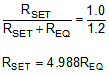
- With REQ of eight parallel, 135Ω ZT (or 16.875Ω equivalent), RSET is 84.5Ω with standard 1% resistor value. IEQ is approximately 11.8 mA. The expected voltage at negative terminals of LVDS ports is approximately 1V. The differential LVDS voltage is 200mV.
- With same RSET of 84.5Ω, if the REQ has dropped to eight parallel, 85Ω ZT (or 10.625Ω equivalent), IEQ is approximately 12.6mA. The expected voltage at negative terminals of LVDS port is approximately 1.06V. The differential LVDS voltage is 138mV. As long as the static LVDS differential voltage is above 100mV, the LVDS port will register a logic HIGH value for the data.
Depending on the DAC3482 functionality required, additional unused LVDS ports such as FRAMEP/N, SYNCP/N, or PARITYP/N can also be left unconnected (floating) or connected to a nominal, differential LVDS active HIGH or active LOW voltage. The usage of these ports depends mainly on the FIFO synchronization settings and parity checking settings. The unused FRAMEP/N, SYNCP/N, or PARITYP/N ports can be connected in parallel with the unused LVDS data port with adjustments to the RSET resistor value.