SLAS751D March 2011 – September 2015 DAC34H84
PRODUCTION DATA.
- 1 Features
- 2 Applications
- 3 Description
- 4 Revision History
- 5 Pin Configuration and Functions
-
6 Specifications
- 6.1 Absolute Maximum Ratings
- 6.2 ESD Ratings
- 6.3 Recommended Operating Conditions
- 6.4 Thermal Information
- 6.5 Electrical Characteristics - DC Specifications
- 6.6 Electrical Characteristics - Digital Specifications
- 6.7 Electrical Characteristics - AC Specifications
- 6.8 Timing Requirements - Digital Specifications
- 6.9 Switching Characteristics - AC Specifications
- 6.10 Typical Characteristics
-
7 Detailed Description
- 7.1 Overview
- 7.2 Functional Block Diagram
- 7.3
Feature Description
- 7.3.1 Serial Interface
- 7.3.2 Data Interface
- 7.3.3 Data Format
- 7.3.4 Input FIFO
- 7.3.5 FIFO Modes of Operation
- 7.3.6 Clocking Modes
- 7.3.7 FIR Filters
- 7.3.8 Complex Signal Mixer
- 7.3.9 Quadrature Modulation Correction (QMC)
- 7.3.10 Temperature Sensor
- 7.3.11 Data Pattern Checker
- 7.3.12 Parity Check Test
- 7.3.13 DAC34H84 Alarm Monitoring
- 7.3.14 LVPECL Inputs
- 7.3.15 LVDS Inputs
- 7.3.16 CMOS Digital Inputs
- 7.3.17 Reference Operation
- 7.3.18 DAC Transfer Function
- 7.3.19 Analog Current Outputs
- 7.4 Device Functional Modes
- 7.5 Programming
- 7.6 Register Map
- 8 Application and Implementation
- 9 Power Supply Recommendations
- 10Layout
- 11Device and Documentation Support
- 12Mechanical, Packaging, and Orderable Information
Package Options
Mechanical Data (Package|Pins)
- ZAY|196
Thermal pad, mechanical data (Package|Pins)
Orderable Information
7 Detailed Description
7.1 Overview
The DAC34H84 includes a quad-channel, 16-bit digital-to-analog converter (DAC) with up to 1.25 GSPS sample rate, a 32-bit LVDS data bus with on-chip termination, FIFO, data pattern checker, and parity test. The device includes 2x to 16x digital interpolation filters with over 90dB of stop-band attenuation, reconstruction filters, independent complex mixers, a low jitter clock multiplier, and digital Quadrature Modulator Correction (QMC).
Full synchronization of multiple devices is possible with the DAC3484. It is an ideal device for next generation communication systems.
7.2 Functional Block Diagram
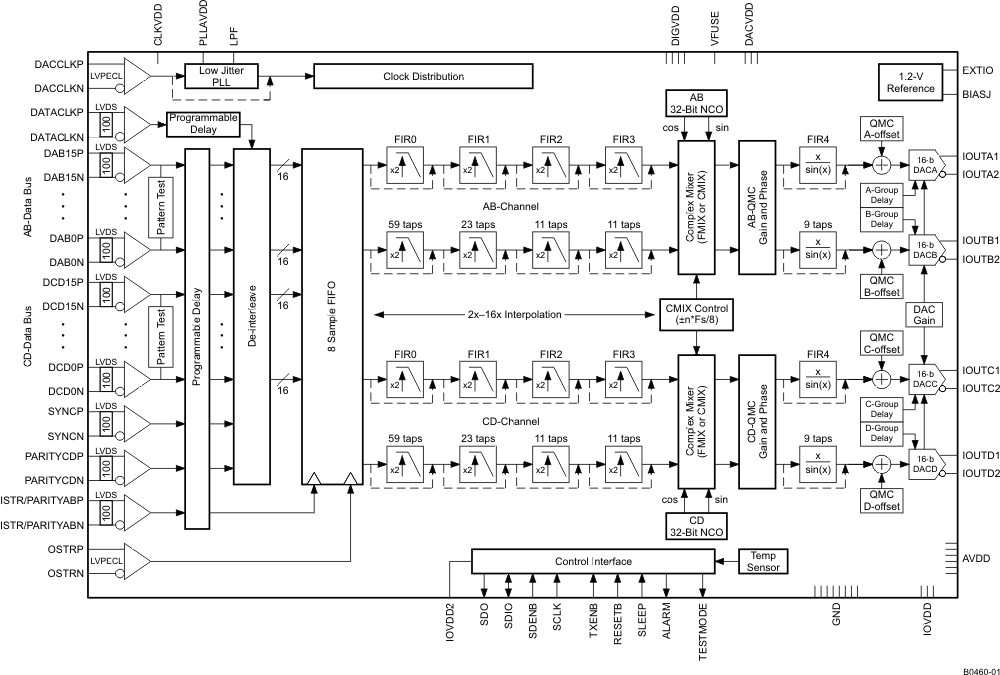
7.3 Feature Description
7.3.1 Serial Interface
The serial port of the DAC34H84 is a flexible serial interface which communicates with industry standard microprocessors and microcontrollers. The interface provides read/write access to all registers used to define the operating modes of DAC34H84. It is compatible with most synchronous transfer formats and can be configured as a 3 or 4 pin interface by sif4_ena in register config2. In both configurations, SCLK is the serial interface input clock and SDENB is serial interface enable. For 3 pin configuration, SDIO is a bidirectional pin for both data in and data out. For 4 pin configuration, SDIO is data in only and SDO is data out only. Data is input into the device with the rising edge of SCLK. Data is output from the device on the falling edge of SCLK.
Each read/write operation is framed by signal SDENB (Serial Data Enable Bar) asserted low. The first frame byte is the instruction cycle which identifies the following data transfer cycle as read or write as well as the 7-bit address to be accessed. Table 1 indicates the function of each bit in the instruction cycle and is followed by a detailed description of each bit. The data transfer cycle consists of two bytes
Table 1. Instruction Byte of the Serial Interface
| BIT | 7 (MSB) | 6 | 5 | 4 | 3 | 2 | 1 | 0 (LSB) |
|---|---|---|---|---|---|---|---|---|
| Description | R/W | A6 | A5 | A4 | A3 | A2 | A1 | A0 |
| R/W | Identifies the following data transfer cycle as a read or write operation. A high indicates a read operation from DAC34H84 and a low indicates a write operation to DAC34H84. |
| [A6 : A0] | Identifies the address of the register to be accessed during the read or write operation. |
Figure 49 shows the serial interface timing diagram for a DAC34H84 write operation. SCLK is the serial interface clock input to DAC34H84. Serial data enable SDENB is an active low input to DAC34H84. SDIO is serial data in. Input data to DAC34H84 is clocked on the rising edges of SCLK.
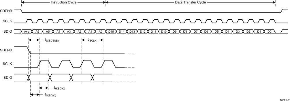 Figure 49. Serial Interface Write Timing Diagram
Figure 50 shows the serial interface timing diagram for a DAC34H84 read operation. SCLK is the serial interface clock input to DAC34H84. Serial data enable SDENB is an active low input to DAC34H84. SDIO is serial data in during the instruction cycle. In 3 pin configuration, SDIO is data out from the DAC34H84 during the data transfer cycle, while SDO is in a high-impedance state. In 4 pin configuration, SDO is data out from the DAC34H84 during the data transfer cycle. At the end of the data transfer, SDIO and SDO will output low on the final falling edge of SCLK until the rising edge of SDENB when it will 3-state.
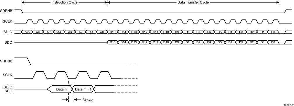 Figure 50. Serial Interface Read Timing Diagram
7.3.2 Data Interface
The DAC34H84 has a 32-bit LVDS bus that accepts quad, 16-bit data in word-wide format. The quad-16-bit data can be input to the device using a dual-bus, 16-bit interface. The bus accepts LVDS transfer rates up to 1.25GSPS which corresponds to a maximum data rate of 625MSPS per data channel. The default LVDS bus input assignment is shown in Table 2.
Table 2. LVDS Bus Input Assignment
| DATA PATHS | PINS |
|---|---|
| A and B | DAB[15..0] |
| C and D | DCD[15..0] |
Data is sampled by the LVDS double data rate (DDR) clock DATACLK. Setup and hold requirements must be met for proper sampling. A and C data are captured on the rising edge of DATACLK. B and D data are captured on the falling edge of DATACLK.
For both input bus modes, a sync signal, either ISTR or SYNC, is required to sync the FIFO read and/or write pointers.
The sync signal, either ISTR or SYNC, can be either a pulse or a periodic signal where the sync period corresponds to multiples of 8 samples. ISTR or SYNC is sampled by a rising edge in DATACLK. The pulse-width t(ISTR_SYNC) needs to be at least equal to 1/2 of the DATACLK period.
7.3.3 Data Format
The 16-bit data for channels A and B is interleaved in the form A0[15:0], B0[15:0], A1[15:0], B1[15:0], A2[15:0]… into the DAB[15:0]P/N LVDS inputs. Similarly data for channels C and D is interleaved into the DCD[15:0]P/N LVDS inputs. Data into the DAC34H84 is formatted according to the diagram shown in Figure 51 where index 0 is the data LSB and index 15 is the data MSB.
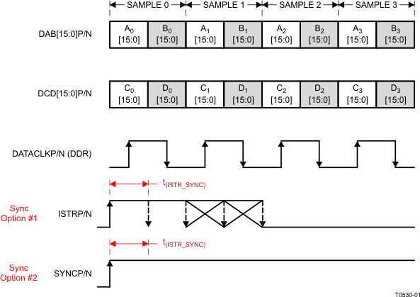 Figure 51. Data Transmission Format
The FIFO read and write pointer can also be synced by SIF SYNC as the third sync option if multi-device synchronization is not needed. In this sync mode, the syncsel_fifoin(3:0) and syncsel_fifoout(3:0) in register config32 need to be both set to 1000b for the SIF SYNC option.
7.3.4 Input FIFO
The DAC34H84 includes a 4-channel, 16-bits wide and 8-samples deep input FIFO which acts as an elastic buffer. The purpose of the FIFO is to absorb any timing variations between the input data and the internal DAC data rate clock such as the ones resulting from clock-to-data variations from the data source.
Figure 52 shows a simplified block diagram of the FIFO.
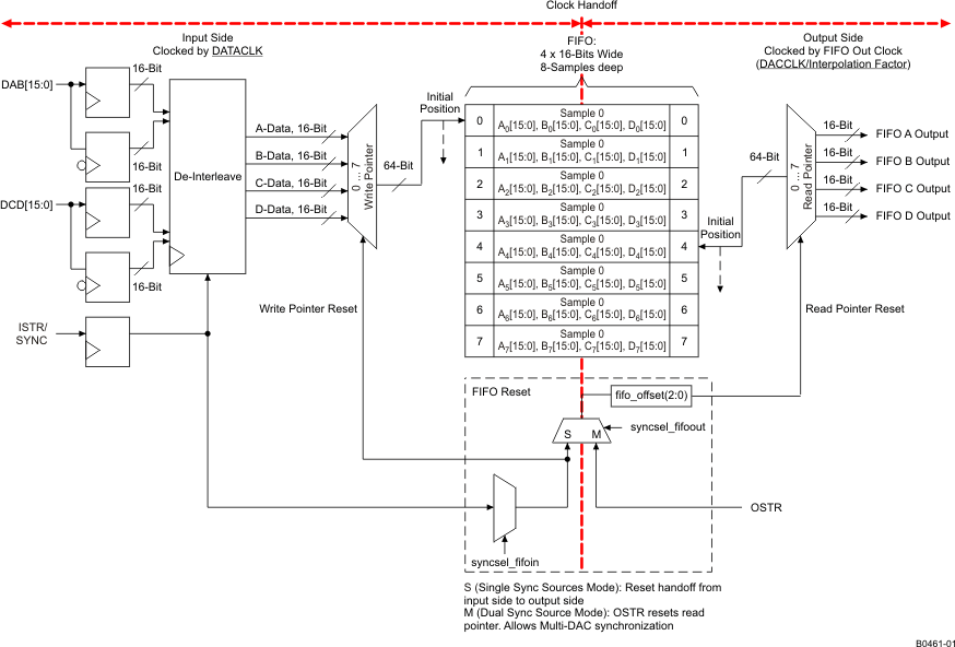 Figure 52. DAC34H84 FIFO Block Diagram
Data is written to the device 32-bits at a time on the rising and falling edges of DATACLK. In order to form a complete 64-bit wide sample (16-bit A-data, 16-bit B-data, 16-bit C-data, and 16-bit D-data) one DATACLK period is required. Each 64-bit wide sample is written into the FIFO at the address indicated by the write pointer. Similarly, data from the FIFO is read by the FIFO Out Clock 64-bits at a time from the address indicated by the read pointer. The FIFO Out Clock is generated internally from the DACCLK signal and its rate is equal to DACCLK/Interpolation. Each time a FIFO write or FIFO read is done the corresponding pointer moves to the next address.
The reset position for the FIFO read and write pointers is set by default to addresses 0 and 4 as shown in Figure 52. This offset gives optimal margin within the FIFO. The default read pointer location can be set to another value using fifo_offset(2:0) in register config3 (address 4 by default). Under normal conditions data is written-to and read-from the FIFO at the same rate and consequently the write and read pointer gap remains constant. If the FIFO write and read rates are different, the corresponding pointers will be cycling at different speeds which could result in pointer collision. Under this condition the FIFO attempts to read and write data from the same address at the same time which will result in errors and thus must be avoided.
The write pointer sync source is selected by syncsel_fifoin(3:0) in register config32. In most applications either ISTR or SYNC are used to reset the write pointer. Unlike DATA, the sync signal is latched only on the rising edges of DATACLK. A rising edge on the sync signal source causes the pointer to return to its original position.
Similarly, the read pointer sync source is selected by syncsel_fifoout(3:0). The write pointer sync source can be set to reset the read pointer as well. In this case, the FIFO Out clock will recapture the write pointer sync signal to reset the read pointer. This clock domain transfer (DATACLK to FIFO Out Clock) results in phase ambiguity of the sync signal. This limits the precise control of the output timing and makes full synchronization of multiple devices difficult.
To alleviate this, the device offers the alternative of resetting the FIFO read pointer independently of the write pointer by using the OSTR signal. The OSTR signal is sampled by DACCLK and must satisfy the timing requirements in the specifications table. In order to minimize the skew it is recommended to use the same clock distribution device such as Texas Instruments CDCE62005 to provide the DACCLK and OSTR signals to all the DAC34H84 devices in the system. Swapping the polarity of the DACCLK outputs with respect to the OSTR ones establishes proper phase relationship.
The FIFO pointers reset procedure can be done periodically or only once during initialization as the pointers automatically return to the initial position when the FIFO has been filled. To reset the FIFO periodically, it is necessary to have the ISTR, SYNC, and OSTR signals to repeat at multiples of 8 FIFO samples. To disable FIFO reset, set syncsel_fifoin(3:0) and syncsel_fifoout(3:0) to “0000”.
The frequency limitation for ISTR and SYNC signals are the following:
fsync = fDATACLK/(n x 8) where n = 1, 2, …
The frequency limitation for the OSTR signal is the following:
fOSTR = fDAC/(n x interpolation x 8) where n = 1, 2, …
The frequencies above are at maximum when n = 1. This is when the ISTR, SYNC, or OSTR have a rising edge transition every 8 FIFO samples. The occurrence can be made less frequent by setting n > 1, for example, every n × 8 FIFO samples.
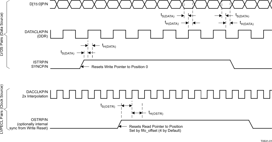 Figure 53. FIFO Write and Read Descriptions
7.3.5 FIFO Modes of Operation
The DAC34H84 input FIFO can be completely bypassed through registers config0 and config32. The register configuration for each mode is described in Table 3.
| Register | Control Bits |
| config0 | fifo_ena |
| config32 | syncsel_fifoout(3:0) |
Table 3. FIFO Operation Modes
| FIFO MODE | config0 AND config32 FIFO BITS | ||||
|---|---|---|---|---|---|
| fifo_ena | syncsel_fifoout | ||||
| BIT 3: sif_sync | BIT 2: OSTR | BIT 1: ISTR | BIT 0: SYNC | ||
| Dual Sync Sources | 1 | 0 | 1 | 0 | 0 |
| Single Sync Source | 1 | 0 | 0 | 1 or 0 Depends on the sync source | 1 or 0 Depends on the sync source |
| Bypass | 0 | X | X | X | X |
7.3.5.1 Dual Sync Sources Mode
This is the recommended mode of operation for those applications that require precise control of the output timing. In Dual Sync Sources mode, the FIFO write and read pointers are reset independently. The FIFO write pointer is reset using the LVDS ISTR or SYNC signal, and the FIFO read pointer is reset using the LVPECL OSTR signal. This allows LVPECL OSTR signal to control the phase of the output for either a single chip or multiple chips. Multiple devices can be fully synchronized in this mode.
7.3.5.2 Single Sync Source Mode
In Single Sync Source mode, the FIFO write and read pointers are reset from the same source, either LVDS ISTR or LVDS SYNC signal. This mode has a possibility of up to 2 DAC clocks offset between the multiple DAC outputs. Applications requiring exact output timing control will need Dual Sync Sources mode instead of Single Sync Source Mode. A single rising edge for FIFO and clock divider sync is recommended. Periodic sync signal is not recommended due to the non-deterministic latency of the sync signal through the clock domain transfer.
In this mode, there is a chance for FIFO pointers 2 away alarm (or possibly 1 away alarm) to occur at initial setup/syncing. This is the result of Single Sync Source mode having 0 to 3 address location slip, which is caused by the asynchronous handoff of the sync signal occurring between the DATACLK zone and DACCLK zone. The asynchronous relationship between the clock domains means there could be a slip (from nominal) in the READ and Write pointers at initial syncing. For example, with the default programming of FIFO Offset of 4, the actual FIFO Offset may be 3, 2, or in some instances, 1. Please note that in this mode, the nominal address location slip is 0 with the possibility getting less for each increase in slip amount. Also, the slip does not continue to occur as the device functions, but the READ/WRITE pointers may not be at optimal settings. In situation of alarm occurrence:
- Adjust the FIFO offset accordingly and resynchronize the FIFO, data formatter, etc such that there are no alarm reported or at least only 2 away alarm is reported.
- The FIFO collision alarm is a warning of the system since the read and write processes occur at the same pointer. However, the FIFO 1 away or 2 away alarms are informational for the system designer. The important thing for these two alarms is that the alarm should not get closer to collision during normal operation. If 1 away alarm and alarm collision starts to occur, it is a warning to check for system errors. The system should have an interrupt or algorithm to fix the error and resynchronize the alarm appropriately.
7.3.5.3 Bypass Mode
In FIFO bypass mode, the FIFO block is not used. As a result the input data is handed off from the DATACLK to the DACCLK domain without any compensation. In this mode the relationship between DATACLK and DACCLK is critical and used as a synchronizing mechanism for the internal logic. Due to this constraint this mode is not recommended. In bypass mode the pointers have no effect on the data path or handoff.
7.3.6 Clocking Modes
The DAC34H84 has a dual clock setup in which a DAC clock signal is used to clock the DAC cores and internal digital logic and a separate DATA clock is used to clock the input LVDS receivers and FIFO input. The DAC34H84 DAC clock signal can be sourced directly or generated through an on-chip low-jitter phase-locked loop (PLL).
In those applications requiring extremely low noise it is recommended to bypass the PLL and source the DAC clock directly from a high-quality external clock to the DACCLK input. In most applications system clocking can be simplified by using the on-chip PLL to generate the DAC core clock while still satisfying performance requirements. In this case the DACCLK pins are used as the reference frequency input to the PLL.
 Figure 54. Top Level Clock Diagram
7.3.6.1 PLL Bypass Mode
In PLL bypass mode a very high quality clock is sourced to the DACCLK inputs. This clock is used to directly source the DAC34H84 DAC sample rate clock. This mode gives the device best performance and is recommended for extremely demanding applications.
The bypass mode is selected by setting the following:
- pll_ena bit in register config24 to 0b to bypass the PLL circuitry.
- pll_sleep bit in register config26 to 1b to put the PLL and VCO into sleep mode.
7.3.6.2 PLL Mode
In this mode the clock at the DACCLKP/N input functions as a reference clock source to the on-chip PLL. The on-chip PLL will then multiply this reference clock to supply a higher frequency DAC sample rate clock. Figure 55 shows the block diagram of the PLL circuit.
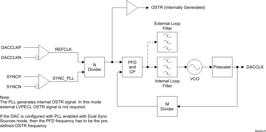 Figure 55. PLL Block Diagram
The DAC34H84 PLL mode is selected by setting the following:
- pll_ena bit in register config24 to 1b to route to the PLL clock path.
- pll_sleep bit in register config26 to 0b to enable the PLL and VCO.
The output frequency of the VCO is designed to be the in the range from 3.3 GHz to 4.0 GHz. The prescaler value, pll_p(2:0) in register config24, should be chosen such that the product of the prescaler value and DAC sample rate clock is within the VCO range. To maintain optimal PLL loop, the coarse tune bits, pll_vco(5:0) in register config26, can adjust the center frequency of the VCO towards the product of the prescaler value and DAC sample rate clock. Figure 56 shows a typical relationship between coarse tune bits and VCO center frequency.
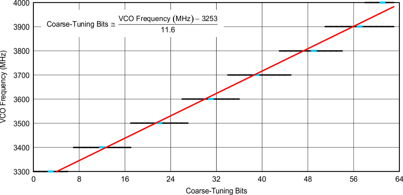 Figure 56. Typical PLL/VCO Lock Range vs Coarse Tuning Bits
Common wireless infrastructure frequencies (614.4 MHz, 737.28 MHz, 983.04 MHz, ...) are generated from this VCO frequency in conjunction with the pre-scaler setting as shown in Table 4.
Table 4. VCO Operation
| VCO FREQUENCY (MHz) | PRE-SCALE DIVIDER | DESIRED DACCLK (MHz) | pll_p(2:0) |
|---|---|---|---|
| 3932.16 | 8 | 491.52 | 111 |
| 3686.4 | 6 | 614.4 | 110 |
| 3686.4 | 5 | 737.28 | 101 |
| 3932.16 | 4 | 983.04 | 100 |
The M divider is used to determine the phase-frequency-detector (PFD) and charge-pump (CP) frequency.
Table 5. PFD and CP Operation
| DACCLK FREQUENCY (MHz) | M DIVIDER | PDF UPDATE RATE (MHz) | pll_m(7:0) |
|---|---|---|---|
| 491.52 | 4 | 122.88 | 00000100 |
| 491.52 | 8 | 61.44 | 00001000 |
| 491.52 | 16 | 30.72 | 00010000 |
| 491.52 | 32 | 15.36 | 00100000 |
The N divider in the loop allows the PFD to operate at a lower frequency than the reference clock. Both M and N dividers can keep the PFD frequency below 155 MHz for peak operation.
The overall divide ratio inside the loop is the product of the Pre-Scale and M dividers (P × M) and the following guidelines should be followed:
- The overall divide ratio range is from 24 to 480
- When the overall divide ratio is less than 120, the internal loop filter can assure a stable loop
- When the overall divide ratio is greater than 120, an external loop filter is required to ensure loop stability
The single charge pump current option is selected by setting pll_cp(1:0) in register config24 to 01b. If an external filter is required, the following filter should be connected to the LPF pin (A1):
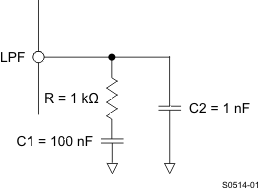 Figure 57. Recommended External Loop Filter
The PLL will generate an internal OSTR signal and does not require the external LVPECL OSTR signal. The OSTR signal is buffered from the N-divider output in the PLL block, and the frequency of the signal is the same as the PFD frequency. Therefore, using PLL with Dual Sync Sources mode would require the PFD frequency to be the pre-defined OSTR frequency. This will allow the FIFO to be synced correctly by the internal OSTR.
7.3.7 FIR Filters
Figure 58 through Figure 61 show the magnitude spectrum response for the FIR0, FIR1, FIR2 and FIR3 interpolating filters where fIN is the input data rate to the FIR filter. Figure 62 to Figure 65 show the composite filter response for 2x, 4x, 8x and 16x interpolation. The transition band for all interpolation settings is from 0.4 to 0.6 x fDATA (the input data rate to the device) with < 0.001dB of pass-band ripple and > 90 dB stop-band attenuation.
The DAC34H84 also has a 9-tap inverse sinc filter (FIR4) that runs at the DAC update rate (fDAC) that can be used to flatten the frequency response of the sample-and-hold output. The DAC sample-and-hold output sets the output current and holds it constant for one DAC clock cycle until the next sample, resulting in the well-known sin(x)/x or sinc(x) frequency response (Figure 66, red line). The inverse sinc filter response (Figure 66, blue line) has the opposite frequency response from 0 to 0.4 x Fdac, resulting in the combined response (Figure 66, green line). Between 0 to 0.4 x fDAC, the inverse sinc filter compensates the sample-and-hold roll-off with less than 0.03 dB error.
The inverse sinc filter has a gain > 1 at all frequencies. Therefore, the signal input to FIR4 must be reduced from full scale to prevent saturation in the filter. The amount of back-off required depends on the signal frequency, and is set such that at the signal frequencies the combination of the input signal and filter response is less than 1 (0 dB). For example, if the signal input to FIR4 is at 0.25 x fDAC, the response of FIR4 is 0.9 dB, and the signal must be backed off from full scale by 0.9 dB to avoid saturation. The gain function in the QMC blocks can be used to reduce the amplitude of the input signal. The advantage of FIR4 having a positive gain at all frequencies is that the user is then able to optimize the back-off of the signal based on its frequency.
The filter taps for all digital filters are listed in Table 3. Note that the loss of signal amplitude may result in lower SNR due to decrease in signal amplitude.
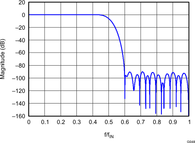 Figure 58. Magnitude Spectrum for FIR0
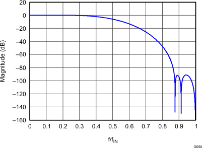 Figure 60. Magnitude Spectrum for FIR2
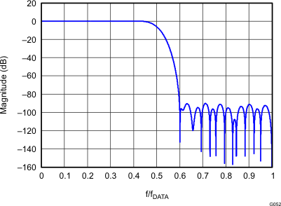 Figure 62. 2x Interpolation Composite Response
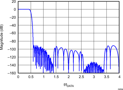 Figure 64. 8x Interpolation Composite Response
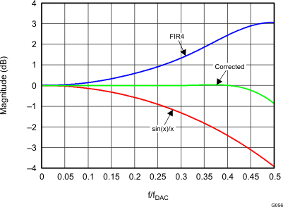 Figure 66. Magnitude Spectrum for Inverse Sinc Filter
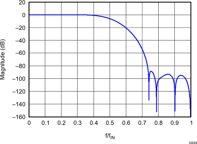 Figure 59. Magnitude Spectrum for FIR1
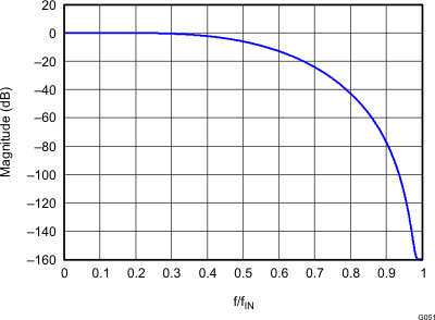 Figure 61. Magnitude Spectrum for FIR3
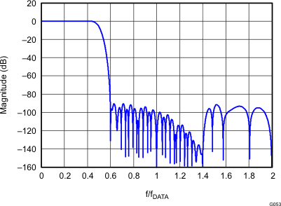 Figure 63. 4x Interpolation Composite Response
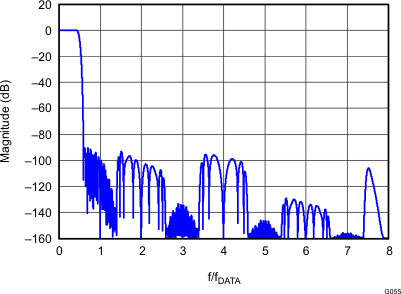 Figure 65. 16x Interpolation Composite Response
Table 6. FIR Filter Coefficients
| INTERPOLATING HALF-BAND FILTERS | NON-INTERPOLATING INVERSE-SINC FILTER | ||||||||
|---|---|---|---|---|---|---|---|---|---|
| FIR0 | FIR1 | FIR2 | FIR3 | FIR4 | |||||
| 59 TAPS | 23 TAPS | 11 TAPS | 11 TAPS | 9 TAPS | |||||
| 6 | 6 | -12 | -12 | 29 | 29 | 3 | 3 | 1 | 1 |
| 0 | 0 | 0 | 0 | 0 | 0 | 0 | 0 | -4 | -4 |
| -19 | -19 | 84 | 84 | -214 | -214 | -25 | -25 | 13 | 13 |
| 0 | 0 | 0 | 0 | 0 | 0 | 0 | 0 | -50 | -50 |
| 47 | 47 | -336 | -336 | 1209 | 1209 | 150 | 150 | 592(1) | |
| 0 | 0 | 0 | 0 | 2048(1) | 256(1) | ||||
| -100 | -100 | 1006 | 1006 | ||||||
| 0 | 0 | 0 | 0 | ||||||
| 192 | 192 | -2691 | -2691 | ||||||
| 0 | 0 | 0 | 0 | ||||||
| -342 | -342 | 10141 | 10141 | ||||||
| 0 | 0 | 16384(1) | |||||||
| 572 | 572 | ||||||||
| 0 | 0 | ||||||||
| -914 | -914 | ||||||||
| 0 | 0 | ||||||||
| 1409 | 1409 | ||||||||
| 0 | 0 | ||||||||
| -2119 | -2119 | ||||||||
| 0 | 0 | ||||||||
| 3152 | 3152 | ||||||||
| 0 | 0 | ||||||||
| -4729 | -4729 | ||||||||
| 0 | 0 | ||||||||
| 7420 | 7420 | ||||||||
| 0 | 0 | ||||||||
| -13334 | -13334 | ||||||||
| 0 | 0 | ||||||||
| 41527 | 41527 | ||||||||
| 65536(1) | |||||||||
7.3.8 Complex Signal Mixer
The DAC34H84 has two paths of complex signal mixer blocks that contain two full complex mixer (FMIX) blocks and power saving coarse mixer (CMIX) blocks. The signal path is shown in Figure 67.
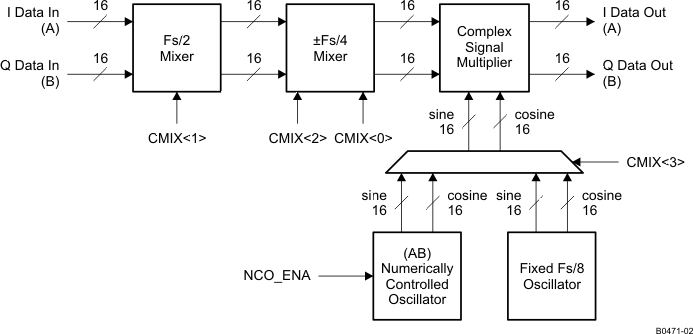
NOTE:
Channel CD data path not shown7.3.8.1 Full Complex Mixer
The two FMIX blocks operate with independent Numerically Controlled Oscillators (NCOs) and enable flexible frequency placement without imposing additional limitations in the signal bandwidth. The NCOs have 32-bit frequency registers (phaseaddAB(31:0) and phaseaddCD(31:0)) and 16-bit phase registers (phaseoffsetAB(15:0) and phaseoffsetCD(15:0)) that generate the sine and cosine terms for the complex mixing. The NCO block diagram is shown in Figure 68.
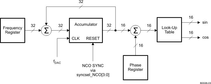 Figure 68. NCO Block Diagram
Synchronization of the NCOs occurs by resetting the NCO accumulators to zero. The synchronization source is selected by syncsel_NCO(3:0) in config31. The frequency word in the phaseaddAB(31:0) and phaseaddCD(31:0) registers is added to the accumulators every clock cycle, fDAC. The output frequency of the NCO is:

With the complex mixer enabled, the two channels in the mixer path are treated as complex vectors of the form IIN(t) + j QIN(t). The complex signal multiplier (shown in Figure 69) will multiply the complex channels with the sine and cosine terms generated by the NCO. The resulting output, IOUT(t) + j QOUT(t), of the complex signal multiplier is:
IOUT(t) = (IIN(t)cos(2πfNCOt + δ) – QIN(t)sin(2πfNCOt + δ)) × 2(mixer_gain – 1)
QOUT(t) = (IIN(t)sin(2πfNCOt + δ) + QIN(t)cos(2πfNCOt + δ)) × 2(mixer_gain – 1)
where t is the time since the last resetting of the NCO accumulator, δ is the phase offset value and mixer_gain is either 0 or 1. δ is given by:
δ = 2π × phase_offsetAB/CD(15:0)/216
The mixer_gain option allows the output signals of the multiplier to reduce by half (6dB). See Mixer Gain section for details.
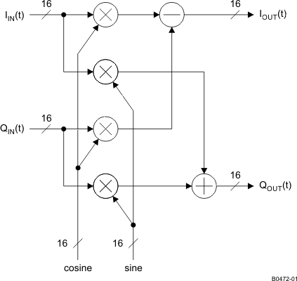 Figure 69. Complex Signal Multiplier
7.3.8.2 Coarse Complex Mixer
In addition to the full complex mixers, the DAC34H84 also has coarse mixer blocks capable of shifting the input signal spectrum by the fixed mixing frequencies ±n×fS/8. Utilizing the coarse mixer instead of the full mixers lowers power consumption.
The output of the fs/2, fs/4, and –fs/4 mixer block is:
IOUT(t) = I(t)cos(2πfCMIXt) – Q(t)sin(2πfCMIXt)
QOUT(t) = I(t)sin(2πfCMIXt) + Q(t)cos(2πfCMIXt)
Since the sine and the cosine terms are a function of fs/2, fs/4, or –fs/4 mixing frequencies, the possible resulting value of the terms will only be 1, -1, or 0. The simplified mathematics allows the complex signal multiplier to be bypassed in any one of the modes, thus mixer gain is not available. The fs/2, fs/4, and –fs/4 mixer blocks performs mixing through negating and swapping of I/Q channel on certain sequence of samples. Table 7 shows the algorithm used for those mixer blocks.
Table 7. Fs/2, Fs/4, and –Fs/4 Mixing Sequence
| MODE | MIXING SEQUENCE |
|---|---|
| Normal (mixer bypassed) | Iout = {+I1, +I2, +I3, +I4…} |
| Qout = {+Q1, +Q2, +Q3, +Q4…} | |
| fs/2 | Iout = {+I1, -I2, +I3, -I4…} |
| Qout = {+Q1, -Q2, +Q3, -Q4…} | |
| fs/4 | Iout = {+I1, -Q2, -I3, +Q4…} |
| Qout = {+Q1, +I2, -Q3, -I4…} | |
| -fs/4 | Iout = {+I1, +Q2, -I3, -Q4…} |
| Qout = {+Q1, -I2, -Q3, +I4…} |
The fs/8 mixer can be enabled along with various combinations of fs/2, fs/4, and –fs/4 mixer. Since the fs/8 mixer uses the complex signal multiplier block with fixed fs/8 sine and cosine term, the output of the multiplier is:
IOUT(t) = (IIN(t)cos(2πfNCOt + δ) – QIN(t)sin(2πfNCOt + δ)) × 2(mixer_gain – 1)
QOUT(t) = (IIN(t)sin(2πfNCOt + δ) + QIN(t)cos(2πfNCOt + δ)) × 2(mixer_gain – 1)
where fCMIX is the fixed mixing frequency selected by cmix(3:0). The mixing combinations are described in Table 8. The mixer_gain option allows the output signals of the multiplier to reduce by half (6dB). See Mixer Gain section for details.
Table 8. Coarse Mixer Combinations
| cmix(3:0) | Fs/8 MIXER cmix(3) |
Fs/4 MIXER cmix(2) |
Fs/2 MIXER cmix(1) |
–Fs/4 MIXER cmix(0) |
MIXING MODE |
|---|---|---|---|---|---|
| 0000 | Disabled | Disabled | Disabled | Disabled | No mixing |
| 0001 | Disabled | Disabled | Disabled | Enabled | –Fs/4 |
| 0010 | Disabled | Disabled | Enabled | Disabled | Fs/2 |
| 0100 | Disabled | Enabled | Disabled | Disabled | +Fs/4 |
| 1000 | Enabled | Disabled | Disabled | Disabled | +Fs/8 |
| 1010 | Enabled | Disabled | Enabled | Disabled | –3Fs/8 |
| 1100 | Enabled | Enabled | Disabled | Disabled | +3Fs/8 |
| 1110 | Enabled | Enabled | Enabled | Disabled | –Fs/8 |
| All others | – | – | – | – | Not recommended |
7.3.8.3 Mixer Gain
The maximum output amplitude out of the complex signal multiplier (i.e., FMIX mode or CMIX mode with fs/8 mixer enabled) occurs if IIN(t) and QIN(t) are simultaneously full scale amplitude and the sine and cosine arguments are equal to 2π x fMIXt + δ (2N-1) x π/4, where N = 1, 2, 3, ....
 Figure 70. Maximum Output of the Complex Signal Multiplier
With mixer_gain = 1 and both IIN(t) and QIN(t) are simultaneously full scale amplitude, the maximum output possible out of the complex signal multiplier is 0.707 + 0.707 = 1.414 (or 3dB). This configuration can cause clipping of the signal and should therefore be used with caution.
With mixer_gain = 0 in config2, the maximum output possible out of the complex signal multiplier is 0.5 x (0.707 + 0.707) = 0.707 (or -3dB). This loss in signal power is in most cases undesirable, and it is recommended that the gain function of the QMC block be used to increase the signal by 3 dB to compensate.
7.3.8.4 Real Channel Upconversion
The mixer in the DAC34H84 treats the A, B, C, and D inputs are complex input data and produces a complex output for most mixing frequencies. The real input data for each channel can be isolated only when the mixing frequency is set to normal mode or fs/2 mode. Refer to Table 7 for details.
7.3.9 Quadrature Modulation Correction (QMC)
7.3.9.1 Gain and Phase Correction
The DAC34H84 includes a Quadrature Modulator Correction (QMC) block. The QMC blocks provide a mean for changing the gain and phase of the complex signals to compensate for any I and Q imbalances present in an analog quadrature modulator. The block diagram for the QMC block is shown in Figure 71. The QMC block contains 3 programmable parameters.
Registers qmc_gainA/B(10:0) and qmc_gainC/D(10:0) controls the I and Q path gains and is an 11-bit unsigned value with a range of 0 to 1.9990 and the default gain is 1.0000. The implied decimal point for the multiplication is between bit 9 and bit 10.
Register qmc_phaseAB/CD(11:0) control the phase imbalance between I and Q and are a 12-bit values with a range of –0.5 to approximately 0.49975. The QMC phase term is not a direct phase rotation but a constant that is multiplied by each "Q" sample then summed into the "I" sample path. This is an approximation of a true phase rotation in order to keep the implementation simple.
LO feed-through can be minimized by adjusting the DAC offset feature described below.
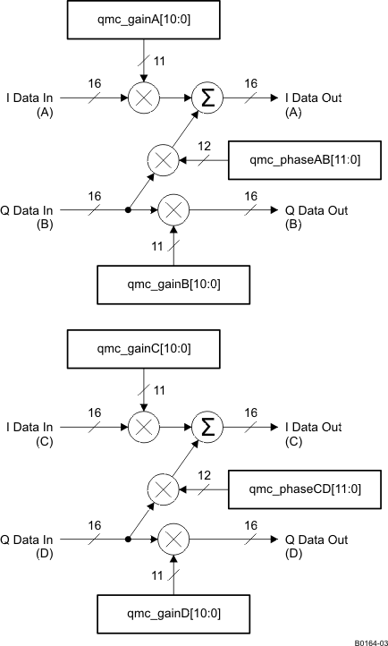 Figure 71. QMC Block Diagram
7.3.9.2 Offset Correction
Registers qmc_offsetA(12:0), qmc_offsetB(12:0), qmc_offsetC(12:0) and qmc_offsetD(12:0) can be used to independently adjust the DC offsets of each channel. The offset values are in represented in 2s-complement format with a range from –4096 to 4095.
The offset value adds a digital offset to the digital data before digital-to-analog conversion. Since the offset is added directly to the data it may be necessary to back off the signal to prevent saturation. Both data and offset values are LSB aligned.
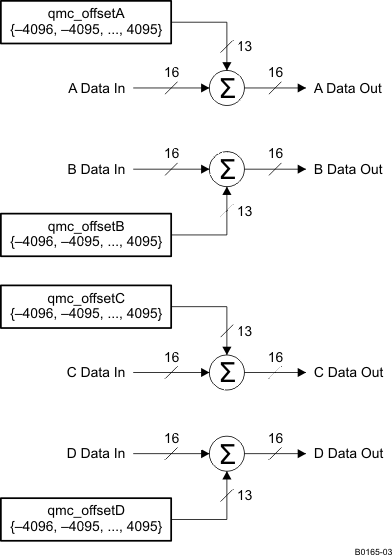 Figure 72. Digital Offset Block Diagram
7.3.9.3 Group Delay Correction
A complex transmitter system typically is consisted of a DAC, reconstruction filter network, and I/Q modulator. Besides the gain and phase mismatch contribution, there could also be timing mismatch contribution from each components. For instance, the timing mismatch could come from the PCB trace length variation between the I and Q channels and the group delay variation from the reconstruction filter.
This timing mismatch in the complex transmitter system creates phase mismatch that varies linearly with respect to frequency. To compensate for the I/Q imbalances due to this mismatch, the DAC34H84 has group delay correction block for each DAC channel. Each DAC channel can adjust its delay through grp_delayA(7:0) grp_delayB(7:0) grp_delayC(7:0) and grp_delayD(7:0) in register config46 and config47. The maximum delay ranges from 30 ps to 100 ps and is dependent on DAC sample clock. Contact TI for specific application information. Refer to the Group Delay vs Step Code plots in the Typical Characteristics section. The group delay correction, along with gain/phase correction, can be useful for correcting imbalances in wide-band transmitter system.
7.3.10 Temperature Sensor
The DAC34H84 incorporates a temperature sensor block which monitors the temperature by measuring the voltage across 2 transistors. The voltage is converted to an 8-bit digital word using a successive-approximation (SAR) analog to digital conversion process. The result is scaled, limited and formatted as a 2s-complement value representing the temperature in degrees Celsius.
The sampling is controlled by the serial interface signals SDENB and SCLK. If the temperature sensor is enabled (tsense_sleep = 0b in register config26) a conversion takes place each time the serial port is written or read. The data is only read and sent out by the digital block when the temperature sensor is read in tempdata(7:0) in config6. The conversion uses the first eight clocks of the serial clock as the capture and conversion clock, the data is valid on the falling eighth SCLK. The data is then clocked out of the chip on the rising edge of the ninth SCLK. No other clocks to the chip are necessary for the temperature sensor operation. As a result the temperature sensor is enabled even when the device is in sleep mode.
In order for the process described above to operate properly, the serial port read from config6 must be done with an SCLK period of at least 1 μs. If this is not satisfied the temperature sensor accuracy is greatly reduced.
7.3.11 Data Pattern Checker
The DAC34H84 incorporates a simple pattern checker test in order to determine errors in the data interface. The main cause of failures is setup/hold timing issues. The test mode is enabled by asserting iotest_ena in register config1. In test mode the analog outputs are deactivated regardless of the state of TXENA or sif_texnable in register config3.
The data pattern key used for the test is 8 words long and is specified by the contents of iotest_pattern[0:7] in registers config37 through config44. The data pattern key can be modified by changing the contents of these registers.
The first word in the test frame is determined by a rising edge transition in ISTR or SYNC, depending on the syncsel_fifoin(3:0) setting in config32. At this transition, the pattern0 word should be input to the data DAB[15:0] pins, and pattern2 should be input to the data DCD[15:0] pins. Patterns 1, 4, and 5 of DAB[15:0] bus and pattern 3, 6, and 7 of DCD[15:0] bus should follow sequentially on each edge of DATACLK (rising and falling). The sequence should be repeated until the pattern checker test is disabled by setting iotest_ena back to 0b. It is not necessary to have a rising ISTR or SYNC edge aligned with every four DATACLK cycle, just the first one to mark the beginning of the series.
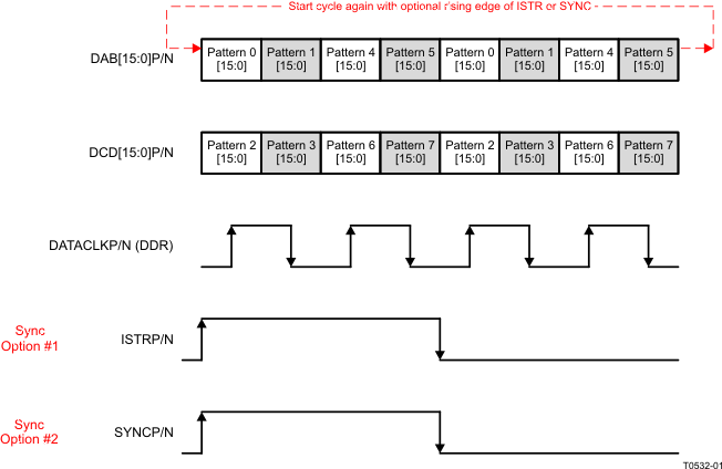 Figure 73. IO Pattern Checker Data Transmission Format
The test mode determines if the all the patterns on the two 16-bit LVDS data buses (DAB[15:0]P/N and DCD[15:0]P/N) were received correctly by comparing the received data against the data pattern key. If any bits in either of the two 16-bit data buses were received incorrectly, the corresponding bits in iotest_results(15:0) in register config4 will be set to 1b to indicate bit error location. The user can check the corresponding bit location on both 16-bit data buses and implement the fix accordingly. Furthermore, the error condition will trigger the alarm_from_iotest bit in register config5 to indicate a general error in the data interface. When data pattern checker mode is enabled, this alarm in register config5, bit7 is the only valid alarm. Other alarms in register config5 are not valid and can be disregarded.
For instance, pattern0 is programmed to the default of 0x7A7A. If the received Pattern 0 is 0x7A7B, then bit 0 in iotest_results(15:0) will be set to 1b to indicate an error in bit 0 location. The alarm_from_iotest will also be set to 1b to report the data transfer error. Note that iotest_results(15:0) does not indicate which of the 16-bit buses has the error. The user needs to check both 16-bit buses and then narrow down the error from the bit location information.
The alarms can be cleared by writing 0x0000 to iotest_results(15:0) and 0b to alarm_from_iotest through the serial interface. The serial interface will read back 0s if there are no errors or if the errors are cleared. The corresponding alarm bit will remain a 1b if the errors remain.
It is recommended to enable the pattern checker and then run the pattern sequence for 100 or more complete cycles before clearing the iotest_results(15:0) and alarm_from_iotest. This will eliminate the possibility of false alarms generated during the setup sequence.
 Figure 74. DAC34H84 Pattern Check Block Diagram
7.3.12 Parity Check Test
The DAC34H84 has a parity check test that enables continuous validity monitoring of the data received by the DAC. Parity check testing in combination with the data pattern checker offer an excellent solution for detecting board assembly issues due to missing pad connections.
For the parity check test, an extra parity bit is added to the data bits to ensure that the total number of set bits (bits with value 1b) is even or odd. This simple scheme is used to detect single or any other odd number of data transfer errors. Parity testing is implemented in the DAC34H84 in two ways: 32-bit parity and dual 16-bit parity.
7.3.12.1 32-Bit Parity
In the 32-bit mode the additional parity bit is sourced to the parity input (PARITYP/N) for the 32-bit data transfer into the DAB[15:0]P/N and DCD[15:0]P/N inputs. This mode is enabled by setting the single_parity_ena bit in register config1. The input parity value is defined to be the total number of logic 1s on the 33-bit data bus – the DAB[15:0]P/N inputs, the DCD[15:0]P/N inputs, and the PARITYP/N input. This value, the total number of logic 1s, must match the parity test selected in the oddeven_parity bit in register config1.
For example, if the oddeven_parity bit is set to 1b for odd parity, then the number of 1s on the 33-bit data bus should be odd. The DAC will check the data transfer through the parity input. If the data received has odd number of 1s, then the parity is correct. If the data received has even number of 1s, then the parity is incorrect. The corresponding alarm for parity error will be set accordingly.
Figure 75 shows the simple XOR structure used to check word parity. Parity is tested independently for data captured on both rising and falling edges of DATACLK (alarm_Aparity and alarm_Bparity, respectively). Testing on both edges helps in determining a possible setup/hold issue. Both alarms are captured individually in register config5.
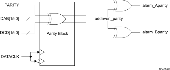 Figure 75. DAC34H84 32-Bit Parity Check
7.3.12.2 Dual 16-Bit Parity
In the dual 16-bit mode, each 16-bit LVDS data bus input will be accompanied by a parity bit for error checking. The DAB[15:0]P/N and ISTRP/N are one 17-bit data path, and the DCD[15:0]P/N and PARITYP/N are another path. This mode is enabled by setting the dual_parity_ena bit in register config1. The input parity value is defined to be the total number of logic 1s on each 17-bit data bus. This value, the total number of logic 1s, must match the parity test selected in the oddeven_parity bit in register config1.
For example, if the oddeven_parity bit is set to 1b for odd parity, then the number of 1s on each 17-bit data bus should be odd. The DAC will check the data transfer through the parity input. If the data received has odd number of 1s, then the parity is correct. If the data received has even number of 1s, then the parity is incorrect. The corresponding alarm for parity error will be set accordingly.
Figure 76 shows the simple XOR structure used to check word parity. Parity is tested independently for data captured on both rising and falling edges of DATACLK for each data path (alarm_Aparity, alarm_Bparity, alarm_Cparity, and alarm_Dparity, respectively). Testing on both edges and both data buses helps in determining a possible setup/hold issue. All of the alarms are captured individually in register config5.
In this mode the ISTR signal functions as a parity signal and cannot be used to sync the FIFO pointer simultaneously. It is recommended to use the SYNC to sync the FIFO pointer. If ISTR has to be used to sync the FIFO pointer, the ISTR sync can only be possible upon start-up when dual 16-bit parity function is disabled. Once the initialization is finished, disable the FIFO pointer sync through ISTR (by configuring syncsel_fifoin and syncsel_fifoout in config32) and enable the dual 16-bit parity function afterwards.
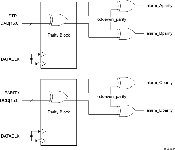 Figure 76. DAC34H84 Dual 16-Bit Parity Check
7.3.13 DAC34H84 Alarm Monitoring
The DAC34H84 includes a flexible set of alarm monitoring that can be used to alert of a possible malfunction scenario. All the alarm events can be accessed either through the config5 register or through the ALARM pin. Once an alarm is set, the corresponding alarm bit in register config5 must be reset through the serial interface to allow further testing. The set of alarms includes the following conditions:
Zero check alarm
- Alarm_from_zerochk. Occurs when the FIFO write pointer has an all zeros pattern. Since the write pointer is a shift register, all zeros will cause the input point to be stuck until the next sync event. When this happens a sync to the FIFO block is required.
FIFO alarms
- alarm_from_fifo. Occurs when there is a collision in the FIFO pointers or a collision event is close.
- alarm_fifo_2away. Pointers are within two addresses of each other.
- alarm_fifo_1away. Pointers are within one address of each other.
- alarm_fifo_collision. Pointers are equal to each other.
Clock alarms
- clock_gone. Occurs when either the DACCLK or DATACLOCK have been stopped.
- alarm_dacclk_gone. Occurs when the DACCLK has been stopped.
- alarm_dataclk_gone. Occurs when the DATACLK has been stopped.
Pattern checker alarm
- alarm_from_iotest. Occurs when the input data pattern does not match the pattern key.
PLL alarm
- alarm_from_pll. Occurs when the PLL is out of lock.
Parity alarms
- alarm_Aparity: In dual parity mode, alarm indicating a parity error on the A word. In single parity mode, alarm on the 32-bit data captured on the rising edge of DATACLKP/N.
- alarm_Bparity: In dual parity mode, alarm indicating a parity error on the B word. In single parity mode, alarm on the 32-bit data captured on the falling edge of DATACLKP/N.
- alarm_Cparity: In dual parity mode, alarm indicating a parity error on the C word.
- alarm_Dparity: In dual parity mode, alarm indicating a parity error on the D word.
To prevent unexpected DAC outputs from propagating into the transmit channel chain, the clock and alarm_ fifo_collision alarms can be set in config2 to shut-off the DAC output automatically regardless of the state of TXENA or sif_txenable.
Alarm monitoring is implemented as follows:
- Power up the device using the recommended power-up sequence.
- Clear all the alarms in config5 by setting them to zeros.
- Unmask those alarms that will generate a hardware interrupt through the ALARM pin in config7.
- Enable automatic DAC shut-off in register config2 if required.
- In the case of an alarm event, the ALARM pin will trigger. If automatic DAC shut-off has been enabled the DAC outputs will be disabled.
- Read registers config5 to determine which alarm triggered the ALARM pin.
- Correct the error condition and re-synchronize the FIFO.
- Clear the alarms in config5.
- Re-read config5 to ensure the alarm event has been corrected.
- Keep clearing and reading config5 until no error is reported.
7.3.14 LVPECL Inputs
Figure 77 shows an equivalent circuit for the DAC input clock (DACCLKP/N) and the output strobe clock (OSTRP/N).
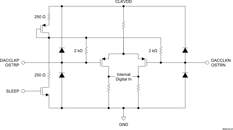 Figure 77. DACCLKP/N and OSTRP/N Equivalent Input Circuit
Figure 78 shows the preferred configuration for driving the CLKIN/CLKINC input clock with a differential ECL/PECL source.
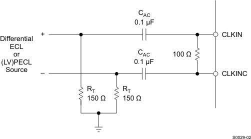 Figure 78. Preferred Clock Input Configuration with a Differential ECL/PECL Clock Source
7.3.15 LVDS Inputs
The DAB[15:0]P/N, DCD[15:0]P/N, DATACLKP/N, SYNCP/N, PARITYP/N, and ISTRP/N LVDS pairs have the input configuration shown in Figure 79. Figure 80 shows the typical input levels and common-move voltage used to drive these inputs.
![DAC34H84 DAB[15:0]P/N,
DCD[15:0]P/N, DATACLKP/N, ISTRP/N, SYNCP/N and PARITYP/N LVDS Input Configuration DAC34H84 S0516-01_LAS748.gif](/ods/images/SLAS751D/S0516-01_LAS748.gif) Figure 79. DAB[15:0]P/N, DCD[15:0]P/N, DATACLKP/N, ISTRP/N, SYNCP/N and PARITYP/N LVDS Input Configuration
Figure 79. DAB[15:0]P/N, DCD[15:0]P/N, DATACLKP/N, ISTRP/N, SYNCP/N and PARITYP/N LVDS Input Configuration
 Figure 80. LVDS Data Input Levels
Table 9. Example LVDS Data Input Levels
| APPLIED VOLTAGES | RESULTING DIFFERENTIAL VOLTAGE | RESULTING COMMON-MODE VOLTAGE | LOGICAL BIT BINARY EQUIVALENT | |
|---|---|---|---|---|
| VA | VB | VA,B | VCOM | |
| 1.4 V | 1.0 V | 400 mV | 1.2 V | 1 |
| 1.0 V | 1.4 V | -400 mV | 0 | |
| 1.2 V | 0.8 V | 400 mV | 1.0 V | 1 |
| 0.8 V | 1.2 V | -400 mV | 0 | |
7.3.16 CMOS Digital Inputs
Figure 81 shows a schematic of the equivalent CMOS digital inputs of the DAC34H84. SDIO, SCLK, SLEEP and TXENA have pull-down resistors while SDENB and RESETB have pull-up resistors internal to the DAC34H84. All the CMOS digital inputs and outputs are referred to the IOVDD2 supply, which can vary from 1.8 V to 3.3 V. This facilitates the I/O interface and eliminates the need of level translation. See the specification table for logic thresholds. The pull-up and pull-down circuitry is approximately equivalent to 100 kΩ.
 Figure 81. CMOS Digital Equivalent Input
7.3.17 Reference Operation
The DAC34H84 uses a bandgap reference and control amplifier for biasing the full-scale output current. The full-scale output current is set by applying an external resistor RBIAS to pin BIASJ. The bias current IBIAS through resistor RBIAS is defined by the on-chip bandgap reference voltage and control amplifier. The default full-scale output current equals 64 times this bias current and can thus be expressed as:
IOUTFS = 64 x IBIAS = 64 x (VEXTIO / RBIAS ) / 2
The DAC34H84 has a 4-bit coarse gain control coarse_dac(3:0) in the config3 register. Using gain control, the IOUTFS can be expressed as:
IOUTFS = (coarse_dac + 1)/16 x IBIAS x 64 = (coarse_dac + 1)/16 x (VEXTIO / RBIAS) / 2 x 64
where VEXTIO is the voltage at terminal EXTIO. The bandgap reference voltage delivers an accurate voltage of 1.2 V. This reference is active when extref_ena = 0b in config27. An external decoupling capacitor CEXT of 0.1 µF should be connected externally to terminal EXTIO for compensation. The bandgap reference can additionally be used for external reference operation. In that case, an external buffer with high impedance input should be applied in order to limit the bandgap load current to a maximum of 100 nA. The internal reference can be disabled and overridden by an external reference by setting the extref_ena control bit. Capacitor CEXT may hence be omitted. Terminal EXTIO thus serves as either input or output node.
The full-scale output current can be adjusted from 30 mA down to 10 mA by varying resistor RBIAS, programming coarse_dac(3:0), or changing the externally applied reference voltage.
NOTE
With internal reference, the minimum Rbias resistor value is 1.28 kΩ. Resistor value below 1.28 kΩ is not recommended since it will program the full-scale current to go above 30 mA and potentially damages the device.
7.3.18 DAC Transfer Function
The CMOS DACs consist of a segmented array of PMOS current sources, capable of sourcing a full-scale output current up to 30 mA. Differential current switches direct the current to either one of the complementary output nodes IOUTP or IOUTN. Complementary output currents enable differential operation, thus canceling out common mode noise sources (digital feed-through, on-chip and PCB noise), dc offsets, even order distortion components, and increasing signal output power by a factor of two.
The full-scale output current is set using external resistor RBIAS in combination with an on-chip bandgap voltage reference source (+1.2 V) and control amplifier. Current IBIAS through resistor RBIAS is mirrored internally to provide a maximum full-scale output current equal to 64 times IBIAS.
The relation between IOUTP and IOUTN can be expressed as:
IOUTFS = IOUTP + IOUTN
We will denote current flowing into a node as – current and current flowing out of a node as + current. Since the output stage is a current source the current flows from the IOUTP and IOUTN pins. The output current flow in each pin driving a resistive load can be expressed as:
IOUTP = IOUTFS x CODE / 65536
IOUTN = IOUTFS x (65535 – CODE) / 65536
where CODE is the decimal representation of the DAC data input word
For the case where IOUTP and IOUTN drive resistor loads RL directly, this translates into single ended voltages at IOUTP and IOUTN:
VOUTP = IOUT1 x RL
VOUTN = IOUT2 x RL
Assuming that the data is full scale (65535 in offset binary notation) and the RL is 25 Ω, the differential voltage between pins IOUTP and IOUTN can be expressed as:
VOUTP = 20mA x 25 Ω = 0.5 V
VOUTN = 0mA x 25 Ω = 0 V
VDIFF = VOUTP – VOUTN = 0.5V
Note that care should be taken not to exceed the compliance voltages at node IOUTP and IOUTN, which would lead to increased signal distortion.
7.3.19 Analog Current Outputs
The DAC34H84 can be easily configured to drive a doubly terminated 50 Ω cable using a properly selected RF transformer. Figure 82 and Figure 83 show the 50 Ω doubly terminated transformer configuration with 1:1 and 4:1 impedance ratio, respectively. Note that the center tap of the primary input of the transformer has to be grounded to enable a DC current flow. Applying a 20 mA full-scale output current would lead to a 0.5 Vpp for a 1:1 transformer and a 1 Vpp output for a 4:1 transformer. The low dc-impedance between IOUTP or IOUTN and the transformer center tap sets the center of the ac-signal to GND, so the 1 Vpp output for the 4:1 transformer results in an output between –0.5 V and +0.5 V.
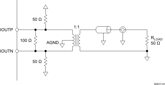 Figure 82. Driving a Doubly Terminated 50-Ω Cable Using a 1:1 Impedance Ratio Transformer
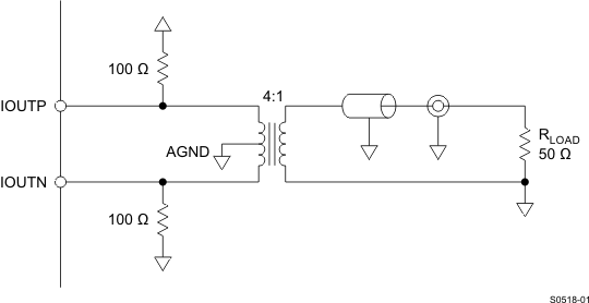 Figure 83. Driving a Doubly Terminated 50-Ω Cable Using a 4:1 Impedance Ratio Transformer
7.4 Device Functional Modes
7.4.1 Multi-Device Synchronization
In various applications, such as multi antenna systems where the various transmit channels information is correlated, it is required that multiple DAC devices are completely synchronized such that their outputs are phase aligned. The DAC34H84 architecture supports this mode of operation.
7.4.1.1 Multi-Device Synchronization: PLL Bypassed with Dual Sync Sources Mode
For single- or multi-device synchronization it is important that delay differences in the data are absorbed by the device so that latency through the device remains the same. Furthermore, to ensure that the outputs from each DAC are phase aligned it is necessary that data is read from the FIFO of each device simultaneously. In the DAC34H84 this is accomplished by operating the multiple devices in Dual Sync Sources mode. In this mode the additional OSTR signal is required by each DAC34H84 to be synchronized.
Data into the device is input as LVDS signals from one or multiple baseband ASICs or FPGAs. Data into multiple DAC devices can experience different delays due to variations in the digital source output paths or board level wiring. These different delays can be effectively absorbed by the DAC34H84 FIFO so that all outputs are phase aligned correctly.
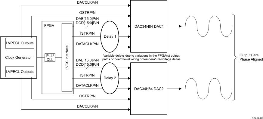 Figure 84. Synchronization System in Dual Sync Sources Mode with PLL Bypassed
For correct operation both OSTR and DACCLK must be generated from the same clock domain. The OSTR signal is sampled by DACCLK and must satisfy the timing requirements in the specifications table. If the clock generator does not have the ability to delay the DACCLK to meet the OSTR timing requirement, the polarity of the DACCLK outputs can be swapped with respect to the OSTR ones to create 180 degree phase delay of the DACCLK. This may help establish proper setup and hold time requirement of the OSTR signal.
Careful board layout planning must be done to ensure that the DACCLK and OSTR signals are distributed from device to device with the lowest skew possible as this will affect the synchronization process. In order to minimize the skew across devices it is recommended to use the same clock distribution device to provide the DACCLK and OSTR signals to all the DAC devices in the system.
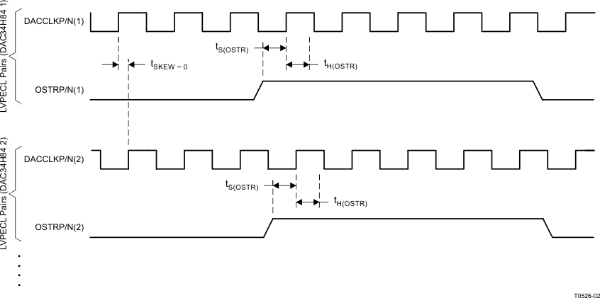 Figure 85. Timing Diagram for LVPECL Synchronization Signals
The following steps are required to ensure the devices are fully synchronized. The procedure assumes all the DAC34H84 devices have a DACCLK and OSTR signal and must be carried out on each device.
- Start-up the device as described in the power-up sequence. Set the DAC34H84 in Dual Sync Sources mode and select OSTR as the clock divider sync source (clkdiv_sync_sel in register config32).
- Sync the clock divider and FIFO pointers.
- Verify there are no FIFO alarms either through register config5 or through the ALARM pin.
- Disable clock divider sync by setting clkdiv_sync_ena to 0b in register config0.
After these steps all the DAC34H84 outputs will be synchronized.
7.4.1.2 Multi-Device Synchronization: PLL Enabled with Dual Sync Sources Mode
The DAC34H84 allows exact phase alignment between multiple devices even when operating with the internal PLL clock multiplier. In PLL clock mode, the PLL generates the DAC clock and an internal OSTR signal from the reference clock applied to the DACCLK inputs so there is no need to supply an additional LVPECL OSTR signal.
For this method to operate properly the SYNC signal should be set to reset the PLL N dividers to a known state by setting pll_ndivsync_ena in register config24 to 1b. The SYNC signal resets the PLL N dividers with a rising edge, and the timing relationship ts(SYNC_PLL) and th(SYNC_PLL) are relative to the reference clock presented on the DACCLK pin.
Both SYNC and DACCLK can be set as low frequency signals to greatly simplifying trace routing (SYNC can be just a pulse as a single rising edge is required, if using a periodic signal it is recommended to clear the pll_ndivsync_ena bit after resetting the PLL dividers). Besides the ts(SYNC_PLL) and th(SYNC_PLL) requirement between SYNC and DACCLK, there is no additional required timing relationship between the SYNC and ISTR signals or between DACCLK and DATACLK. The only restriction as in the PLL disabled case is that the DACCLK and SYNC signals are distributed from device to device with the lowest skew possible.
 Figure 86. Synchronization System in Dual Sync Sources Mode with PLL Enabled
The following steps are required to ensure the devices are fully synchronized. The procedure assumes all the DAC34H84 devices have a DACCLK and OSTR signal and must be carried out on each device.
- Start-up the device as described in the power-up sequence. Set the DAC34H84 in Dual Sync Sources mode and enable SYNC to reset the PLL dividers (set pll_ndivsync_ena in register config24 to 1b).
- Reset the PLL dividers with a rising edge on SYNC.
- Disable PLL dividers resetting.
- Sync the clock divider and FIFO pointers.
- Verify there are no FIFO alarms either through register config5 or through the ALARM pin.
- Disable clock divider sync by setting clkdiv_sync_ena to 0b in register config0.
After these steps all the DAC34H84 outputs will be synchronized.
7.4.1.3 Multi-Device Operation: Single Sync Source Mode
In Single Sync Source mode, the FIFO write and read pointers are reset from the same sync source, either ISTR or SYNC. Although the FIFO in this mode can still absorb the data delay differences due to variations in the digital source output paths or board level wiring it is impossible to guarantee data will be read from the FIFO of different devices simultaneously thus preventing exact phase alignment.
In Single Sync Source mode the FIFO read pointer reset is handoff between the two clock domains (DATACLK and FIFO OUT CLOCK) by simply re-sampling the write pointer reset. Since the two clocks are asynchronous there is a small but distinct possibility of a meta-stability during the pointer handoff. This meta-stability can cause the outputs of the multiple devices to slip by up to 2 DAC clock cycles.
When the PLL is enabled with Single Sync Source mode, the FIFO read pointer is not synchronized by the OSTR signal. Therefore, there is no restriction on the PLL PFD frequency as described in the previous section.
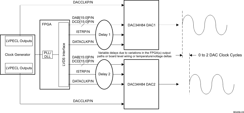 Figure 87. Multi-Device Operation in Single Sync Source Mode
7.5 Programming
7.5.1 Power-Up Sequence
The following startup sequence is recommended to power-up the DAC34H84:
- Set TXENA low
- Supply all 1.2-V voltages (DACVDD, DIGVDD, CLKVDD and VFUSE) and all 3.3-V voltages (AVDD, IOVDD, and PLLAVDD). The 1.2-V and 3.3-V supplies can be powered up simultaneously or in any order. There are no specific requirements on the ramp rate for the supplies.
- Provide all LVPECL inputs: DACCLKP/N and the optional OSTRP/N. These inputs can also be provided after the SIF register programming.
- Toggle the RESETB pin for a minimum 25 ns active low pulse width.
- Program the SIF registers.
- Program fuse_sleep (config27, bit<11>) to put the internal fuses to sleep.
- FIFO configuration needed for synchronization:
- Program syncsel_fifoin(3:0) (config32, bit<15:12>) to select the FIFO input pointer sync source.
- Program syncsel_fifoout(3:0) (config32, bit<11:8>) to select the FIFO output pointer sync source.
- Program syncsel_fifo_input(1:0) (config31, bit<3:2>) to select the FIFO input sync source.
- Clock divider configuration needed for synchronization:
- Program clkdiv_sync_sel (config32, bit<0>) to select the clock divider sync source.
- Program clkdiv_sync_ena (config0, bit<2>) to 1b to enable clock divider sync.
- For multi-DAC synchronization in PLL mode, program pll_ndivsync_ena (config24, bit<11>) to 1b to synchronize the PLL N-divider.
- Provide all LVDS inputs (D[15:0]P/N, DCD[15:0]P/N, DATACLKP/N, ISTRP/N, SYNCP/N and PARITYP/N) simultaneously. Synchronize the FIFO and clock divider by providing the pulse or periodic signals needed.
- For Single Sync Source Mode where either ISTRP/N or SYNCP/N is used to sync the FIFO, a single rising edge for FIFO and clock divider sync is recommended. Periodic sync signal is not recommended due to the non-deterministic latency of the sync signal through the clock domain transfer.
- For Dual Sync Sources Mode, both single pulse or periodic sync signals can be used.
- For multi-DAC synchronization in PLL mode, the LVDS SYNCP/N signal is used to sync the PLL N-divider and can be sourced from either the FPGA/ASIC pattern generator or clock distribution circuit as long as the t(SYNC_PLL) setup and hold timing requirement is met with respect to the reference clock source at DACCLKP/N pins. The LVDS SYNCP/N signal can be provided at this point.
- FIFO and clock divider configurations after all the sync signals have provided the initial sync pulses needed for synchronization:
- For Single Sync Source Mode where the clock divider sync source is either ISTRP/N or SYNCP/N, clock divider syncing must be disabled after DAC34H84 initialization and before the data transmission by setting clkdiv_sync_ena (config0, bit 2) to 0b.
- For Dual Sync Sources Mode, where the clock divider sync source is from the OSTR signal (either from external OSTRP/N or internal PLL N divider output), the clock divider syncing may be enabled at all time.
- Optionally, to prevent accidental syncing of the FIFO when sending the ISTRP/N or SYNCP/N pulse to other digital blocks such as NCO, QMC, ..., disable FIFO syncing by setting syncsel_fifoin(3:0) and syncsel_fifoout(3:0) to 0000b after the FIFO input and output pointers are initialized. If the FIFO and sync remain enabled after initialization, the ISTRP/N or SYNCP/N pulse must occur in ways to not disturb the FIFO operation. Refer to the INPUT FIFO section for detail.
- Disable PLL N-divider syncing by setting pll_ndivsync_ena (config24, bit<11>) to 0b.
- Enable transmit of data by asserting the TXENA pin or set sif_txenable to 1b.
- At any time, if any of the clocks (for example, DATACLK or DACCLK) is lost or a FIFO collision alarm is detected, a complete resynchronization of the DAC is necessary. Set TXENABLE low and repeat steps 7 through 11. Program the FIFO configuration and clock divider configuration per steps 7 and 8 appropriately to accept the new sync pulse or pulses for the synchronization.
7.5.2 Example Start-Up Routine
7.5.2.1 Device Configuration
| fDATA = 491.52 MSPS | |||
| Interpolation = 2x | |||
| Input data = baseband data | |||
| fOUT = 122.88 MHz | |||
| PLL = Enabled | |||
| Full Mixer = Enabled | |||
| Dual Sync Sources Mode |
7.5.2.2 PLL Configuration
| fREFCLK = 491.52 MHz at the DACCLKP/N LVPECL pins | |||
| fDACCLK = fDATA x Interpolation = 983.04 MHz | |||
| fVCO = 4 x fDACCLK = 3932.16 MHz (keep fVCO between 3.3 GHz to 4 GHz) | |||
| PFD = fOSTR = 30.72 MHz | |||
| N = 16, M = 32, P = 4, single charge pump | |||
| pll_vco(5:0) = 111011b (59) |
7.5.2.3 NCO Configuration
| fNCO = 122.88 MHz | |||
| fNCO_CLK = 983.04 MHz | |||
| freq = fNCO x 2^32 / 983.04 = 536870912 = 0x20000000 | |||
| phaseaddAB(31:0) or phaseaddCD(31:0) = 0x20000000 | |||
| NCO SYNC = sif_sync |
7.5.2.4 Example Start-Up Sequence
Table 10. Example Start-Up Sequence Description
| STEP | READ/WRITE | ADDRESS | VALUE | DESCRIPTION |
|---|---|---|---|---|
| 1 | N/A | N/A | N/A | Set TXENA Low |
| 2 | N/A | N/A | N/A | Power-up the device |
| 3 | N/A | N/A | N/A | Apply LVPECL DACCLKP/N for PLL reference clock |
| 4 | N/A | N/A | N/A | Toggle RESETB pin |
| 5 | Write | 0x00 | 0xF19F | QMC offset and correction enabled, 2x int, FIFO enabled, Alarm enabled, clock divider sync enabled, inverse sinc filter enabled. |
| 6 | Write | 0x01 | 0x040E | Single parity enabled, FIFO alarms enabled (2 away, 1 away, and collision). |
| 7 | Write | 0x02 | 0x7052 | Output shut-off when DACCLK gone, DATACLK gone, and FIFO collision. Mixer block with NCO enabled, twos complement. |
| 8 | Write | 0x03 | 0xA000 | Output current set to 20 mAFS with internal reference and 1.28-kΩ RBIAS resistor. |
| 9 | Write | 0x07 | 0xD8FF | Un-mask FIFO collision, DACCLK-gone, and DATACLK-gone alarms to the Alarm output. |
| 10 | Write | 0x08 | N/A | Program the desired channel A QMC offset value. (Causes Auto-Sync for QMC AB-Channels Offset Block) |
| 11 | Write | 0x09 | N/A | Program the desired FIFO offset value and channel B QMC offset value. |
| 12 | Write | 0x0A | N/A | Program the desired channel C QMC offset value. (Causes Auto-Sync for QMC CD-Channels Offset Block) |
| 13 | Write | 0x0B | N/A | Program the desired channel D QMC offset value. |
| 14 | Write | 0x0C | N/A | Program the desired channel A QMC gain value. |
| 15 | Write | 0x0D | N/A | Coarse mixer mode not used. Program the desired channel B QMC gain value. |
| 16 | Write | 0x0E | N/A | Program the desired channel B QMC gain value. |
| 17 | Write | 0x0F | N/A | Program the desired channel C QMC gain value. |
| 18 | Write | 0x10 | N/A | Program the desired channel AB QMC phase value. (Causes Auto-Sync QMC AB-Channels Correction Block) |
| 19 | Write | 0x11 | N/A | Program the desired channel CD QMC phase value. (Causes Auto-Sync for the QMC CD-Channels Correction Block) |
| 20 | Write | 0x12 | N/A | Program the desired channel AB NCO phase offset value. (Causes Auto-Sync for Channel AB NCO Mixer) |
| 21 | Write | 0x13 | N/A | Program the desired channel CD NCO phase offset value. (Causes Auto-Sync for Channel CD NCO Mixer) |
| 22 | Write | 0x14 | 0x2000 | Program the desired channel AB NCO frequency value |
| 23 | Write | 0x15 | 0x0000 | Program the desired channel AB NCO frequency value |
| 24 | Write | 0x16 | 0x2000 | Program the desired channel CD NCO frequency value |
| 25 | Write | 0x17 | 0x0000 | Program the desired channel CD NCO frequency value |
| 26 | Write | 0x18 | 0x2C67 | PLL enabled, PLL N-dividers sync enabled, single charge pump, prescaler = 4. |
| 27 | Write | 0x19 | 0x20F4 | M = 32, N = 16, PLL VCO bias tune = 01b |
| 28 | Write | 0x1A | 0xEC00 | PLL VCO coarse tune = 59 |
| 29 | Write | 0x1B | 0x0800 | Internal reference |
| 30 | Write | 0x1E | 0x9999 | QMC offset AB, QMC offset CD, QMC correction AB, and QMC correction CD can be synced by sif_sync or auto-sync from register write |
| 31 | Write | 0x1F | 0x4440 | Mixer AB and CD values synced by SYNCP/N. NCO accumulator synced by SYNCP/N. |
| 32 | Write | 0x20 | 0x2400 | FIFO Input Pointer Sync Source = ISTR FIFO Output Pointer Sync Source = OSTR (from PLL N-divider output) Clock Divider Sync Source = OSTR |
| 33 | N/A | N/A | N/A | Provide all the LVDS DATA and DATACLK Provide rising edge ISTRP/N and rising edge SYNCP/N to sync the FIFO input pointer and PLL N-dividers. |
| 34 | Read | 0x18 | N/A | Read back pll_lfvolt(2:0). If the value is not optimal, adjust pll_vco(5:0) in 0x1A. |
| 35 | Write | 0x05 | 0x0000 | Clear all alarms in 0x05. |
| 36 | Read | 0x05 | N/A | Read back all alarms in 0x05. Check for PLL lock, FIFO collision, DACCLK-gone, DATACLK-gone, .... Fix the error appropriately. Repeat step 34 and 35 as necessary. |
| 37 | Write | 0x1F | 0x4442 | Sync all the QMC blocks using sif_sync. These blocks can also be synced via auto-sync through appropriate register writes. |
| 38 | Write | 0x00 | 0xF19B | Disable clock divider sync. |
| 39 | Write | 0x1F | 0x4448 | Set sif_sync to 0b for the next sif_sync event. |
| 40 | Write | 0x20 | 0x0000 | Disable FIFO input and output pointer sync. |
| 41 | Write | 0x18 | 0x2467 | Disable PLL N-dividers sync. |
| 42 | N/A | N/A | N/A | Set TXENA high. Enable data transmission. |
7.6 Register Map
Table 11. Register Map(1)
7.6.1 Register Descriptions
Table 12. Register Name: config0 – Address: 0x00, Default: 0x049C
| Register Name | Address | Bit | Name | Function | Default Value | |
|---|---|---|---|---|---|---|
| config0 | 0x00 | 15 | qmc_offsetAB_ena | When set, the digital Quadrature Modulator Correction (QMC) offset correction for the AB data path is enabled. | 0 | |
| 14 | qmc_offsetCD_ena | When set, the digital Quadrature Modulator Correction (QMC) offset correction for the CD data path is enabled. | 0 | |||
| 13 | qmc_corrAB_ena | When set, the QMC phase and gain correction circuitry for the AB data path is enabled. | 0 | |||
| 12 | qmc_corrCD_ena | When set, the QMC phase and gain correction circuitry for the CD data path is enabled. | 0 | |||
| 11:8 | interp(3:0) | These bits define the interpolation factor | 0100 | |||
| interp | Interpolation Factor | |||||
| 0000 | 1x | |||||
| 0001 | 2x | |||||
| 0010 | 4x | |||||
| 0100 | 8x | |||||
| 1000 | 16x | |||||
| 7 | fifo_ena | When set, the FIFO is enabled. When the FIFO is disabled DACCCLKP/N and DATACLKP/N must be aligned (not recommended). | 1 | |||
| 6 | Reserved | Reserved for factory use. | 0 | |||
| 5 | Reserved | Reserved for factory use. | 0 | |||
| 4 | alarm_out_ena | When set, the ALARM pin becomes an output. When cleared, the ALARM pin is 3-stated. | 1 | |||
| 3 | alarm_out_pol | This bit changes the polarity of the ALARM signal. MM 0: Negative logic MM 1: Positive logic |
1 | |||
| 2 | clkdiv_sync_ena | When set, enables the syncing of the clock divider and the FIFO output pointer using the sync source selected by register config32. The internal divided-down clocks will be phase aligned after syncing. Refer to the Power-Up Sequence section for more detail. | 1 | |||
| 1 | invsincAB_ena | When set, the inverse sinc filter for the AB data path is enabled. | 0 | |||
| 0 | invsincCD_ena | When set, the inverse sinc filter for the CD data path is enabled. | 0 | |||
Table 13. Register Name: config1 – Address: 0x01, Default: 0x040E
| Register Name | Address | Bit | Name | Function | Default Value |
|---|---|---|---|---|---|
| config1 | 0x01 | 15 | iotest_ena | When set, enables the data pattern checker test. The outputs are deactivated regardless of the state of TXENA and sif_txenable. | 0 |
| 14 | Reserved | Reserved for factory use. | 0 | ||
| 13 | Reserved | Reserved for factory use. | 0 | ||
| 12 | 64cnt_ena | When set, enables resetting of the alarms after 64 good samples with the goal of removing unnecessary errors. For instance, when checking setup/hold through the pattern checker test, there may initially be errors. Setting this bit removes the need for a SIF write to clear the alarm register. | 0 | ||
| 11 | oddeven_parity | Selects between odd and even parity check MM 0: Even parity MM 1: Odd parity |
0 | ||
| 10 | single_parity_ena | When set, enables parity checking of each input word using the 1 PARITYP/N parity input. It should match the oddeven_parity register setting. | 1 | ||
| 9 | dual_parity_ena | When set, enables parity checking using the ISTR signal to 0 source the parity bit. The parity bit should match the oddeven_parity register setting. | 0 | ||
| 8 | rev_interface | When set, the PARITY, SYNC, and ISTR inputs are rotated to allow complete reversal of the data interface when setting the rev_interface bit. When rev_interface = 1b, the following changes occurs MM 1. SYNCP/N becomes ISTRP/N MM 2. PARITYP/N becomes SYNCP/N MM 3. ISTRP/N becomes PARITYP/N |
0 | ||
| 7 | dacA_complement | When set, the DACA output is complemented. This allows to effectively change the + and – designations of the LVDS data lines. | 0 | ||
| 6 | dacB_complement | When set, the DACB output is complemented. This allows to effectively change the + and – designations of the LVDS data lines. | 0 | ||
| 5 | dacC_complement | When set, the DACC output is complemented. This allows to effectively change the + and – designations of the LVDS data lines. | 0 | ||
| 4 | dacD_complement | When set, the DACD output is complemented. This allows to effectively change the + and – designations of the LVDS data lines. | 0 | ||
| 3 | alarm_2away_ena | When set, the alarm from the FIFO indicating the write and read pointers being 2 away is enabled. | 1 | ||
| 2 | alarm_1away_ena | When set, the alarm from the FIFO indicating the write and read pointers being 1 away is enabled. | 1 | ||
| 1 | alarm_collision_ena | When set, the alarm from the FIFO indicating a collision between the write and read pointers is enabled. | 1 | ||
| 0 | Reserved | Reserved for factory use. | 0 |
Table 14. Register Name: config2 – Address: 0x02, Default: 0x7000
| Register Name | Address | Bit | Name | Function | Default Value |
|---|---|---|---|---|---|
| config2 | 0x02 | 15 | Reserved | Reserved for factory use. | 0 |
| 14 | dacclkgone_ena | When set, the DACCLK-gone signal from the clock monitor circuit can be used to shut off the DAC outputs. The corresponding alarms, alarm_dacclk_gone and alarm_output_gone, must not be masked (for example, Config7, bit <10> and bit <8> must set to 0b). | 1 | ||
| 13 | dataclkgone_ena | When set, the DATACLK-gone signal from the clock monitor circuit can be used to shut off the DAC outputs. The corresponding alarms, alarm_dataclk_gone and alarm_output_gone, must not be masked (for example, Config7, bit <9> and bit <8> must set to 0b). | 1 | ||
| 12 | collisiongone_ena | When set, the FIFO collision alarms can be used to shut off the DAC outputs. The corresponding alarms, alarm_fifo_collision and alarm_output_gone, must not be masked (for example, Config7, bit <13> and bit <8> must set to 0b). | 1 | ||
| 11 | Reserved | Reserved for factory use. | 0 | ||
| 10 | Reserved | Reserved for factory use. | 0 | ||
| 9 | Reserved | Reserved for factory use. | 0 | ||
| 8 | Reserved | Reserved for factory use. | 0 | ||
| 7 | sif4_ena | When set, the serial interface (SIF) is a 4 bit interface, otherwise it is a 3-bit interface. | 0 | ||
| 6 | mixer_ena | When set, the mixer block is enabled. | 0 | ||
| 5 | mixer_gain | When set, a 6dB gain is added to the mixer output. | 0 | ||
| 4 | nco_ena | When set, the NCO is enabled. This is not required for coarse mixing. | 0 | ||
| 3 | revbus | When set, the input bits for the data bus are reversed. MSB becomes LSB. | 0 | ||
| 2 | Reserved | Reserved for factory use. | 0 | ||
| 1 | twos | When set, the input data format is expected to be 2s-complement. When cleared, the input is expected to be offset-binary. | 0 | ||
| 0 | Reserved | Reserved for factory use. | 0 |
Table 15. Register Name: config3 – Address: 0x03, Default: 0xF000
| Register Name | Address | Bit | Name | Function | Default Value |
|---|---|---|---|---|---|
| config3 | 0x03 | 15:12 | coarse_dac(3:0) | Scales the output current in 16 equal steps. | 1111 |
 |
|||||
| 11:8 | Reserved | Reserved for factory use. | 0000 | ||
| 7:1 | Reserved | Reserved for factory use. | 0000000 | ||
| 0 | sif_txenable | When set, the internal value of TXENABLE is set to 1b. To enable analog output data transmission, set sif_txenable to 1b or pull CMOS TXENA pin (N9) to high. To disable analog output, set sif_txenable to 0b and pull CMOS TXENA pin (N9) to low. |
0 |
Table 16. Register Name: config4 – Address: 0x04, Default: No RESET Value (Write to Clear)
| Register Name | Address | Bit | Name | Function | Default Value |
|---|---|---|---|---|---|
| config4 | 0x04 | 15:0 | iotest_results(15:0) | Bits in iotest_results with logic value of 1b tell which bit in either DAB[15:0] bus or DCD[15:0] bus failed during the pattern checker test. iotest_results(15:8) correspond to the data bits on both DAB[15:8] and DCD[15:8]. iotest_results(7:0) correspond to the data bits on both DAB[7:0] and DCD[7:0]. |
No RESET Value |
Table 17. Register Name: config5 – Address: 0x05, Default: Setup and Power-Up Conditions Dependent (Write to Clear)
| Register Name | Address | Bit | Name | Function | Default Value |
|---|---|---|---|---|---|
| config5 | 0x05 | 15 | alarm_from_zerochk | This alarm indicates the 8-bit FIFO write pointer address has an all zeros patterns. Due to pointer address being a shift register, this is not a valid address and will cause the write pointer to be stuck until the next sync. This error is typically caused by timing error or improper power start-up sequence. If this alarm is asserted, resynchronization of FIFO is necessary. Refer to the Power-Up Sequence section for more detail. | NA |
| 14 | Reserved | Reserved for factory use. | NA | ||
| 13:11 | alarms_from_fifo(2:0) | Alarm indicating FIFO pointer collisions and nearness: MM 000: All fine MM 001: Pointers are 2 away MM 01x: Pointers are 1 away MM 1xx: FIFO pointer collision If the FIFO pointer collision alarm is set when collisiongone_ena is enabled, the FIFO must be re-synchronized and the bits must be cleared to resume normal operation. |
NA | ||
| 10 | alarm_dacclk_gone | Alarm indicating the DACCLK has been stopped. If the bit is set when dacclkgone_ena is enabled, the DACCLK must resume and the bit must be cleared to resume normal operation. |
NA | ||
| 9 | alarm_dataclk_gone | Alarm indicating the DATACLK has been stopped. If the bit is set when dataclkgone_ena is enabled, the DATACLK must resume and the bit must be cleared to resume normal operation. |
NA | ||
| 8 | alarm_output_gone | Alarm indicating either alarm_dacclk_gone, alarm_dataclk_gone, or alarm_fifo_collision are asserted. It controls the output. When high it will output 0x8000 for each output connected to the DAC. If the bit is set when dacclkgone_ena, dataclkgone_ena, or collisiongone_ena are enabled, then the corresponding errors must be fixed and the bits must be cleared to resume normal operation. | NA | ||
| 7 | alarm_from_iotest | Alarm indicating the input data pattern does not match the pattern in the iotest_pattern registers. When data pattern checker mode is enabled, this alarm in register config5, bit7 is the only valid alarm. Other alarms in register config5 are not valid and can be disregarded. | NA | ||
| 6 | Reserved | Reserved for factory use. | NA | ||
| 5 | alarm_from_pll | Alarm indicating the PLL has lost lock. For version ID 001, alarm_from_PLL may not indicate the correct status of the PLL. Refer to pll_lfvolt(2:0) in register config24 for proper PLL lock indication. | NA | ||
| 4 | alarm_Aparity | In dual parity mode, alarm indicating a parity error on the A word. In single parity mode, alarm on the 32-bit data captured on the rising edge of DATACLKP/N. | NA | ||
| 3 | alarm_Bparity | In dual parity mode, alarm indicating a parity error on the B word. In single parity mode, alarm on the 32-bit data captured on the falling edge of DATACLKP/N. | NA | ||
| 2 | alarm_Cparity | In dual parity mode, alarm indicating a parity error on the C word. | NA | ||
| 1 | alarm_Dparity | In dual parity mode, alarm indicating a parity error on the D word. | NA | ||
| 0 | Reserved | Reserved for factory use. | NA |
Table 18. Register Name: config6 – Address: 0x06, Default: No RESET Value (Read Only)
| Register Name | Address | Bit | Name | Function | Default Value |
|---|---|---|---|---|---|
| config6 | 0x06 | 15:8 | tempdata(7:0) | This is the output from the chip temperature sensor. The value of this register in two’s complement format represents the temperature in degrees Celsius. This register must be read with a minimum SCLK period of 1μs. | No RESET Value |
| 7:2 | Reserved | Reserved for factory use. | 000000 | ||
| 1 | Reserved | Reserved for factory use. | 0 | ||
| 0 | Reserved | Reserved for factory use. | 0 |
Table 19. Register Name: config7 – Address: 0x07, Default: 0xFFFF
| Register Name | Address | Bit | Name | Function | Default Value | |
|---|---|---|---|---|---|---|
| config7 | 0x07 | 15:0 | alarms_mask(15:0) | These bits control the masking of the alarms. (0=not masked, 1= masked) | 0xFFFF | |
| alarm_mask | Alarm that is Masked | |||||
| 15 | alarm_from_zerochk | |||||
| 14 | not used | |||||
| 13 | alarm_fifo_collision | |||||
| 12 | alarm_fifo_1away | |||||
| 11 | alarm_fifo_2away | |||||
| 10 | alarm_dacclk_gone | |||||
| 9 | alarm_dataclk_gone | |||||
| 8 | alarm_output_gone | |||||
| 7 | alarm_from_iotest | |||||
| 6 | not used | |||||
| 5 | alarm_from_pll | |||||
| 4 | alarm_Aparity | |||||
| 3 | alarm_Bparity | |||||
| 2 | alarm_Cparity | |||||
| 1 | alarm_Dparity | |||||
| 0 | not used | |||||
Table 20. Register Name: config8 – Address: 0x08, Default: 0x0000 (Causes Auto-Sync)
| Register Name |
Address | Bit | Name | Function | Default Value |
|---|---|---|---|---|---|
| config8 | 0x08 | 15 | Reserved | Reserved for factory use. | 0 |
| 14 | Reserved | Reserved for factory use. | 0 | ||
| 13 | Reserved | Reserved for factory use. | 0 | ||
| 12:0 | qmc_offsetA(12:0) | DACA offset correction. The offset is measured in DAC LSBs. If enabled in config30 writing to this register causes an auto-sync to be generated. This loads the values of the QMC offset registers (config8-config9) into the offset block at the same time. When updating the offset values for the AB channel config8 should be written last. Programming config9 will not affect the offset setting. | All zeros |
Table 21. Register Name: config9 – Address: 0x09, Default: 0x8000
| Register Name |
Address | Bit | Name | Function | Default Value |
|---|---|---|---|---|---|
| config9 | 0x09 | 15:13 | fifo_offset(2:0) | When the sync to the FIFO occurs, this is the value loaded into the FIFO read pointer. With this value the initial difference between write and read pointers can be controlled. This may be helpful in syncing multiple chips or controlling the delay through the device. | 100 |
| 12:0 | qmc_offsetB(12:0) | DACB offset correction. The offset is measured in DAC LSBs. | All zeros |
Table 22. Register Name: config10 – Address: 0x0A, Default: 0x0000 (Causes Auto-Sync)
| Register Name |
Address | Bit | Name | Function | Default Value |
|---|---|---|---|---|---|
| config10 | 0x0A | 15 | Reserved | Reserved for factory use. | 0 |
| 14 | Reserved | Reserved for factory use. | 0 | ||
| 13 | Reserved | Reserved for factory use. | 0 | ||
| 12:0 | qmc_offsetC(12:0) | DACC offset correction. The offset is measured in DAC LSBs. If enabled in config30 writing to this register causes an auto-sync to be generated. This loads the values of the CD-channel QMC offset registers (config10-config11) into the offset block at the same time. When updating the offset values for the CD-channel config10 should be written last. Programming config11 will not affect the offset setting. | All zeros |
Table 23. Register Name: config11 – Address: 0x0B, Default: 0x0000
| Register Name |
Address | Bit | Name | Function | Default Value |
|---|---|---|---|---|---|
| config11 | 0x0B | 15 | Reserved | Reserved for factory use. | 0 |
| 14 | Reserved | Reserved for factory use. | 0 | ||
| 13 | Reserved | Reserved for factory use. | 0 | ||
| 12:0 | qmc_offsetD(12:0) | DACD offset correction. The offset is measured in DAC LSBs. | All zeros |
Table 24. Register Name: config12 – Address: 0x0C, Default: 0x0400
| Register Name |
Address | Bit | Name | Function | Default Value |
|---|---|---|---|---|---|
| config12 | 0x0C | 15 | Reserved | Reserved for factory use. | 0 |
| 14 | Reserved | Reserved for factory use. | 0 | ||
| 13 | Reserved | Reserved for factory use. | 0 | ||
| 12 | Reserved | Reserved for factory use. | 0 | ||
| 11 | Reserved | Reserved for factory use. | 0 | ||
| 10:0 | qmc_gainA(10:0) | QMC gain for DACA. The full 11-bit qmc_gainA(10:0) word is formatted as UNSIGNED with a range of 0 to 1.9990. The implied decimal point for the multiplication is between bit 9 and bit 10. | 10000000000 |
Table 25. Register Name: config13 – Address: 0x0D, Default: 0x0400
| Register Name |
Address | Bit | Name | Function | Default Value |
|---|---|---|---|---|---|
| config13 | 0x0D | 15 | cmix_mode(3:0) | Sets the mixing function of the coarse mixer. MM Bit 15: Fs/8 mixer MM Bit 14: Fs/4 mixer MM Bit 13: Fs/2 mixer MM Bit 12: -Fs/4 mixer The various mixers can be combined together to obtain a ±n×Fs/8 total mixing factor. |
0000 |
| 11 | Reserved | Reserved for factory use. | 0 | ||
| 10:0 | qmc_gainB(10:0) | QMC gain for DACB. The full 11-bit qmc_gainB(10:0) word is formatted as UNSIGNED with a range of 0 to 1.9990. The implied decimal point for the multiplication is between bit 9 and bit 10. | 10000000000 |
Table 26. Register Name: config14 – Address: 0x0E, Default: 0x0400
| Register Name |
Address | Bit | Name | Function | Default Value |
|---|---|---|---|---|---|
| config14 | 0x0E | 15 | Reserved | Reserved for factory use. | 0 |
| 14 | Reserved | Reserved for factory use. | 0 | ||
| 13 | Reserved | Reserved for factory use. | 0 | ||
| 12 | Reserved | Reserved for factory use. | 0 | ||
| 11 | Reserved | Reserved for factory use. | 0 | ||
| 10:0 | qmc_gainC(10:0) | QMC gain for DACC. The full 11-bit qmc_gainC(10:0) word is formatted as UNSIGNED with a range of 0 to 1.9990. The implied decimal point for the multiplication is between bit 9 and bit 10. | 10000000000 |
Table 27. Register Name: config15 – Address: 0x0F, Default: 0x0400
| Register Name |
Address | Bit | Name | Function | Default Value |
|---|---|---|---|---|---|
| config15 | 0x0F | 15:14 | output_ delayAB(1:0) | Delays the AB data path outputs from 0 to 3 DAC clock cycles. | 00 |
| 13:12 | output_ delayCD(1:0) | Delays the CD data path outputs from 0 to 3 DAC clock cycles. | 00 | ||
| 11 | Reserved | Reserved for factory use. | 0 | ||
| 10:0 | qmc_gainD(10:0) | QMC gain for DACD. The full 11-bit qmc_gainD(10:0) word is formatted as UNSIGNED with a range of 0 to 1.9990. The implied decimal point for the multiplication is between bit 9 and bit 10. | 10000000000 |
Table 28. Register Name: config16 – Address: 0x10, Default: 0x0000 (Causes Auto-Sync)
| Register Name |
Address | Bit | Name | Function | Default Value |
|---|---|---|---|---|---|
| config16 | 0x10 | 15 | Reserved | Reserved for factory use. | 0 |
| 14 | Reserved | Reserved for factory use. | 0 | ||
| 13 | Reserved | Reserved for factory use. | 0 | ||
| 12 | Reserved | Reserved for factory use. | 0 | ||
| 11:0 | qmc_phaseAB(11:0) | QMC correction phase for the AB data path. The 12-bit qmc_phaseAB(11:0) word is formatted as two’s complement and scaled to occupy a range of -0.5 to 0.49975 and a default phase correction of 0.00. To accomplish QMC phase correction, this value is multiplied by the current B sample, then summed into the A sample. If enabled in config30 writing to this register causes an auto-sync to be generated. This loads the values of the QMC offset registers (config12, config13, and config16) into the QMC block at the same time. When updating the QMC values for the AB channel config16 should be written last. Programming config12 and config13 will not affect the QMC settings. | All zeros |
Table 29. Register Name: config17 – Address: 0x11, Default: 0x0000 (Causes Auto-Sync)
| Register Name |
Address | Bit | Name | Function | Default Value |
|---|---|---|---|---|---|
| config17 | 0x11 | 15 | Reserved | Reserved for factory use. | 0 |
| 14 | Reserved | Reserved for factory use. | 0 | ||
| 13 | Reserved | Reserved for factory use. | 0 | ||
| 12 | Reserved | Reserved for factory use. | 0 | ||
| 11:0 | qmc_phaseCD(11:0) | QMC correction phase for the CD data path. The 12-bit qmc_gainCD(11:0) word is formatted as two’s complement and scaled to occupy a range of -0.5 to 0.49975 and a default phase correction of 0.00. To accomplish QMC phase correction, this value is multiplied by the current D sample, then summed into the C sample. If enabled in config30 writing to this register causes an auto-sync to be generated. This loads the values of the CD-channel QMC block registers (config14, config15 and config17) into the QMC block at the same time. When updating the QMC values for the CD-channel config17 should be written last. Programming config14 and config15 will not affect the QMC settings. | All zeros |
Table 30. Register Name: config18 – Address: 0x12, Default: 0x0000 (Causes Auto-Sync)
| Register Name |
Address | Bit | Name | Function | Default Value |
|---|---|---|---|---|---|
| config18 | 0x12 | 15:0 | phase_offsetAB(15:0) | Phase offset added to the AB data path NCO accumulator before the generation of the SIN and COS values. The phase offset is added to the upper 16 bits of the NCO accumulator results and these 16 bits are used in the sin/cos lookup tables. If enabled in config31 writing to this register causes an auto-sync to be generated. This loads the values of the fine mixer block registers (config18, config20, and config21) at the same time. When updating the mixer values the config18 should be written last. Programming config20 and config21 will not affect the mixer settings. | 0x0000 |
Table 31. Register Name: config19 – Address: 0x13, Default: 0x0000 (Causes Auto-Sync)
| Register Name |
Address | Bit | Name | Function | Default Value |
|---|---|---|---|---|---|
| config19 | 0x13 | 15:0 | phase_offsetCD(15:0) | Phase offset added to the CD data path NCO accumulator before the generation of the SIN and COS values. The phase offset is added to the upper 16 bits of the NCO accumulator results and these 16 bits are used in the sin/cos lookup tables. If enabled in config31 writing to this register causes an auto-sync to be generated. This loads the values of the CD-channel fine mixer block registers (config19, config22, and config23) at the same time. When updating the mixer values for the CD-channel config19 should be written last. Programming config22 and config23 will not affect the mixer settings. | 0x0000 |
Table 32. Register Name: config20 – Address: 0x14, Default: 0x0000
| Register Name |
Address | Bit | Name | Function | Default Value |
|---|---|---|---|---|---|
| config20 | 0x14 | 15:0 | phase_ addAB(15:0) | The phase_addAB(15:0) value is used to determine the NCO frequency. The two’s complement formatted value can be positive or negative. Each LSB represents Fs/(2^32) frequency step. | 0x0000 |
Table 33. Register Name: config21 – Address: 0x15, Default: 0x0000
| Register Name |
Address | Bit | Name | Function | Default Value |
|---|---|---|---|---|---|
| config21 | 0x15 | 15:0 | phase_ addAB(31:16) | See config20 above. | 0x0000 |
Table 34. Register Name: config22 – Address: 0x16, Default: 0x0000
| Register Name |
Address | Bit | Name | Function | Default Value |
|---|---|---|---|---|---|
| config22 | 0x16 | 15:0 | phase_ addCD(15:0) | The phase_addCD(15:0) value is used to determine the NCO frequency. The 2s-complement formatted value can be positive or negative. Each LSB represents Fs/(2^32) frequency step. | 0x0000 |
Table 35. Register Name: config23 – Address: 0x17, Default: 0x0000
| Register Name |
Address | Bit | Name | Function | Default Value |
|---|---|---|---|---|---|
| config23 | 0x17 | 15:0 | phase_ addCD(31:16) | See config22 above. | 0x0000 |
Table 36. Register Name: config24 – Address: 0x18, Default: NA
| Register Name |
Address | Bit | Name | Function | Default Value |
|---|---|---|---|---|---|
| config24 | 0x18 | 15:13 | Reserved | Reserved for factory use. | 001 |
| 12 | pll_reset | When set, the PLL loop filter (LPF) is pulled down to 0V. Toggle from 1b to 0b to restart the PLL if an over-speed lock-up occurs. Over-speed can happen when the process is fast, the supplies are higher than nominal, .... resulting in the feedback dividers missing a clock. | 0 | ||
| 11 | pll_ndivsync_ena | When set, the LVDS SYNC input is used to sync the PLL N dividers. | 1 | ||
| 10 | pll_ena | When set, the PLL is enabled. When cleared, the PLL is bypassed. | 0 | ||
| 9:8 | Reserved | Reserved for factory use. | 00 | ||
| 7:6 | pll_cp(1:0) | PLL pump charge select MM 00: No charge pump MM 01: Single pump charge MM 10: Not used MM 11: Dual pump charge |
00 | ||
| 5:3 | pll_p(2:0) | PLL pre-scaler dividing module control. MM 010: 2 MM 011: 3 MM 100: 4 MM 101: 5 MM 110: 6 MM 111: 7 MM 000: 8 |
001 | ||
| 2:0 | pll_lfvolt(2:0) | PLL loop filter voltage. This three bit read-only indicator has step size of 0.4125 V. The entire range covers from 0 V to 3.3 V. The optimal lock range of the PLL will be from 010 to 101 (for example, 0.825 V to 2.063 V). Adjust pll_vco(5:0) for optimal lock range. | NA |
Table 37. Register Name: config25 – Address: 0x19, Default: 0x0440
| Register Name |
Address | Bit | Name | Function | Default Value |
|---|---|---|---|---|---|
| config25 | 0x19 | 15:8 | pll_m(7:0) | M portion of the M/N divider of the PLL. If pll_m<7> = 0, the M divider value has the range of pll_m<6:0>, spanning from 4 to 127. (for example, 0, 1, 2, and 3 are not valid.) If pll_m<7> = 1, the M divider value has the range of 2 × pll_m<6:0>, spanning from 8 to 254. (for example, 0, 2, 4, and 6 are not valid. M divider has even values only.) |
0x04 |
| 7:4 | pll_n(3:0) | N portion of the M/N divider of the PLL. MM 0000: 1 MM 0001: 2 MM 0010: 3 MM 0011: 4 MM 0100: 5 MM 0101: 6 MM 0110: 7 MM 0111: 8 MM 1000: 9 MM 1001: 10 MM 1010: 11 MM 1011: 12 MM 1100: 13 MM 1101: 14 MM 1110: 15 MM 1111: 16 |
0100 | ||
| 3:2 | pll_vcoitune(1:0) | PLL VCO bias tuning bits. Set to 01b for normal PLL operation | 00 | ||
| 1:0 | Reserved | Reserved for factory use. | 00 |
Table 38. Register Name: config26 – Address: 0x1A, Default: 0x0020
| Register Name |
Address | Bit | Name | Function | Default Value |
|---|---|---|---|---|---|
| config26 | 0x1A | 15:10 | pll_vco(5:0) | VCO frequency coarse tuning bits. | 000000 |
| 9 | Reserved | Reserved for factory use. | 0 | ||
| 8 | Reserved | Reserved for factory use. | 0 | ||
| 7 | bias_sleep | When set, the bias amplifier is put into sleep mode. | 0 | ||
| 6 | tsense_sleep | Turns off the temperature sensor when asserted. | 0 | ||
| 5 | pll_sleep | When set, the PLL is put into sleep mode. | 1 | ||
| 4 | clkrecv_sleep | When asserted the clock input receiver gets put into sleep mode. This affects the OSTR receiver as well. | 0 | ||
| 3 | sleepA | When set, the DACA is put into sleep mode. | 0 | ||
| 2 | sleepB | When set, the DACB is put into sleep mode. | 0 | ||
| 1 | sleepC | When set, the DACC is put into sleep mode. | 0 | ||
| 0 | sleepD | When set, the DACD is put into sleep mode. | 0 |
Table 39. Register Name: config27 – Address: 0x1B, Default: 0x0000
| Register Name |
Address | Bit | Name | Function | Default Value | |||
|---|---|---|---|---|---|---|---|---|
| config27 | 0x1B | 15 | extref_ena | Allows the device to use an external reference or the internal reference. 0: Internal reference 1: External reference |
0 | |||
| 14 | Reserved | Reserved for factory use. | 0 | |||||
| 13 | Reserved | Reserved for factory use. | 0 | |||||
| 12 | Reserved | Reserved for factory use. | 0 | |||||
| 11 | fuse_sleep | Put the fuses to sleep when set high. Note: Default value is 0b. Must be set to 1b for proper operation |
0 | |||||
| 10 | Reserved | Reserved for factory use. | 0 | |||||
| 9 | Reserved | Reserved for factory use. | 0 | |||||
| 8 | Reserved | Reserved for factory use. | 0 | |||||
| 7 | Reserved | Reserved for factory use. | 0 | |||||
| 6 | Reserved | Reserved for factory use. | 0 | |||||
| 5:0 | atest | ATEST mode allows the user to check for the internal die voltages to ensure the supply voltages are within the range. When ATEST mode is programmed, the internal die voltages can be measured at the TXENA pin. The TXENA pin (N9) must be floating without any pull-up or pull-down resistors. In ATEST mode, the TXENA and sif_txenable logics are bypassed, and output will be active at all time. |
000000 | |||||
| Config27, bit<5:0> | Description | Expected Nominal Voltage | ||||||
| 001110 | DACA AVSS | 0 V | ||||||
| 001111 | DACA DVDD | 1.2 V | ||||||
| 010000 | DACA AVDD | 3.3 V | ||||||
| 010110 | DACB AVSS | 0 V | ||||||
| 010111 | DACB DVDD | 1.2 V | ||||||
| 011000 | DACB AVDD | 3.3 V | ||||||
| 011110 | DACC AVSS | 0 V | ||||||
| 011111 | DACC DVDD | 1.2 V | ||||||
| 100000 | DACC AVDD | 3.3 V | ||||||
| 100110 | DACD AVSS | 0 V | ||||||
| 100111 | DACD DVDD | 1.2 V | ||||||
| 101000 | DACD AVDD | 3.3 V | ||||||
| 110000 | 1.2VDIG | 1.2 V | ||||||
| 000101 | 1.2VCLK | 1.2 V | ||||||
Table 40. Register Name: config28 – Address: 0x1C, Default: 0x0000
| Register Name |
Address | Bit | Name | Function | Default Value |
|---|---|---|---|---|---|
| config28 | 0x1C | 15:8 | Reserved | Reserved for factory use. | 0x00 |
| 7:0 | Reserved | Reserved for factory use. | 0x00 |
Table 41. Register Name: config29 – Address: 0x1D, Default: 0x0000
| Register Name |
Address | Bit | Name | Function | Default Value |
|---|---|---|---|---|---|
| config29 | 0x1D | 15:8 | Reserved | Reserved for factory use. | 0x00 |
| 7:0 | Reserved | Reserved for factory use. | 0x00 |
Table 42. Register Name: config30 – Address: 0x1E, Default: 0x1111
| Register Name |
Address | Bit | Name | Function | Default Value |
|---|---|---|---|---|---|
| config30 | 0x1E | 15:12 | syncsel_qmoffsetAB(3:0) | Selects the syncing source(s) of the AB data path double buffered QMC offset registers. A 1b in the bit enables the signal as a sync source. More than one sync source is permitted. MM Bit 15: sif_sync (via config31) MM Bit 14: SYNC MM Bit 13: OSTR MM Bit 12: Auto-sync from register write |
0001 |
| 11:8 | syncsel_qmoffsetCD(3:0) | Selects the syncing source(s) of the CD data path double buffered QMC offset registers. A 1b in the bit enables the signal as a sync source. More than one sync source is permitted. MM Bit 11: sif_sync (via config31) MM Bit 10: SYNC MM Bit 9: OSTR MM Bit 8: Auto-sync from register write |
0001 | ||
| 7:4 | syncsel_qmcorrAB(3:0) | Selects the syncing source(s) of the AB data path double buffered QMC offset registers. A 1b in the bit enables the signal as a sync source. More than one sync source is permitted. MM Bit 7: sif_sync (via config31) MM Bit 6: SYNC MM Bit 5: OSTR MM Bit 4: Auto-sync from register write |
0001 | ||
| 3:0 | syncsel_qmcorrCD(3:0) | Selects the syncing source(s) of the CD data path double buffered QMC offset registers. A 1b in the bit enables the signal as a sync source. More than one sync source is permitted. MM Bit 3: sif_sync (via config31) MM Bit 2: SYNC MM Bit 1: OSTR MM Bit 0: Auto-sync from register write |
0001 |
Table 43. Register Name: config31 – Address: 0x1F, Default: 0x1140
| Register Name |
Address | Bit | Name | Function | Default Value |
|---|---|---|---|---|---|
| config31 | 0x1F | 15:12 | syncsel_mixerAB(3:0) | Selects the syncing source(s) of the AB data path double buffered mixer registers. A 1b in the bit enables the signal as a sync source. More than one sync source is permitted. MM Bit 15: sif_sync (via config31) MM Bit 14: SYNC MM Bit 13: OSTR MM Bit 12: Auto-sync from register write |
0001 |
| 11:8 | syncsel_mixerCD(3:0) | Selects the syncing source(s) of the CD data path double buffered mixer registers. A 1b in the bit enables the signal as a sync source. More than one sync source is permitted. MM Bit 11: sif_sync (via config31) MM Bit 10: SYNC MM Bit 9: OSTR MM Bit 8: Auto-sync from register write |
0001 | ||
| 7:4 | syncsel_nco(3:0) | Selects the syncing source(s) of the two NCO accumulators. A 1b in the bit enables the signal as a sync source. More than one sync source is permitted. MM Bit 7: sif_sync (via config31) MM Bit 6: SYNC MM Bit 5: OSTR MM Bit 4: ISTR |
0100 | ||
| 3:2 | syncsel_fifo_input | Selects either ISTR or SYNC LVDS signal to be routed to the internal FIFO_ISTR path if syncsel_fifoin(3:0) is set to be ISTR (for example, syncsel_fifoin(3:0) = 0010b). In conjunction with config1 register bit(8), this allows flexibility of external LVDS signal routing to the internal FIFO. The syncsel_fifo_input(1:0) can only have one bit active at a time. MM 00: external LVDS ISTR signal to internal FIFO_ISTR path MM 01: external LVDS SYNC signal to internal FIFO_ISTR path MM 10: external LVDS ISTR signal to internal FIFO_ISTR path MM 11: external LVDS SYNC signal to internal FIFO_ISTR path |
00 | ||
| 1 | sif_sync | SIF created sync signal. Set to 1b to cause a sync and then clear to 0b to remove it. | 0 | ||
| 0 | Reserved | Reserved for factory use. | 0 |
Table 44. Register Name: config32 – Address: 0x20, Default: 0x2400
Table 45. Register Name: config33 – Address: 0x21, Default: 0x0000
| Register Name |
Address | Bit | Name | Function | Default Value |
|---|---|---|---|---|---|
| config33 | 0x21 | 15:0 | Reserved | Reserved for factory use. | 0x0000 |
Table 46. Register Name: config34 – Address: 0x22, Default: 0x1B1B
| Register Name |
Address | Bit | Name | Function | Default Value |
|---|---|---|---|---|---|
| config34 | 0x22 | 15:14 | pathA_in_sel(1:0) | Selects the word used for the A channel path. | 00 |
| 13:12 | pathB_in_sel(1:0) | Selects the word used for the B channel path. | 01 | ||
| 11:10 | pathC_in_sel(1:0) | Selects the word used for the C channel path. | 10 | ||
| 9:8 | pathD_in_sel(1:0) | Selects the word used for the D channel path. | 11 | ||
| 7:6 | DACA_out_sel(1:0) | Selects the word used for the DACA output. | 00 | ||
| 5:4 | DACB_out_sel(1:0) | Selects the word used for the DACB output. | 01 | ||
| 3:2 | DACC_out_sel(1:0) | Selects the word used for the DACC output. | 10 | ||
| 1:0 | DACD_out_sel(1:0) | Selects the word used for the DACD output. | 11 |
Table 47. Register Name: config35 – Address: 0x23, Default: 0xFFFF
Table 48. Register Name: config36 – Address: 0x24, Default: 0x0000
| Register Name |
Address | Bit | Name | Function | Default Value |
|---|---|---|---|---|---|
| config36 | 0x24 | 15:13 | datadly(2:0) | Controls the delay of the data inputs through the LVDS receivers. Each LSB adds approximately 50 ps 0: Minimum |
000 |
| 12:10 | clkdly(2:0) | Controls the delay of the data clock through the LVDS receivers. Each LSB adds approximately 50 ps 0: Minimum |
000 | ||
| 9:0 | Reserved | Reserved for factory use. | 0x000 |
Table 49. Register Name: config37 – Address: 0x25, Default: 0x7A7A
| Register Name |
Address | Bit | Name | Function | Default Value |
|---|---|---|---|---|---|
| config37 | 0x25 | 15:0 | iotest_pattern0 | Dataword0 in the IO test pattern. It is used with the seven other words to test the input data. At the start of the IO test pattern, this word should be aligned with rising edge of ISTR or SYNC signal to indicate sample 0. |
0x7A7A |
Table 50. Register Name: config38 – Address: 0x26, Default: 0xB6B6
| Register Name |
Address | Bit | Name | Function | Default Value |
|---|---|---|---|---|---|
| config38 | 0x26 | 15:0 | iotest_pattern1 | Dataword1 in the IO test pattern. It is used with the seven other words to test the input data. | 0xB6B6 |
Table 51. Register Name: config39 – Address: 0x27, Default: 0xEAEA
| Register Name |
Address | Bit | Name | Function | Default Value |
|---|---|---|---|---|---|
| config39 | 0x27 | 15:0 | iotest_pattern2 | Dataword2 in the IO test pattern. It is used with the seven other words to test the input data. | 0xEAEA |
Table 52. Register Name: config40 – Address: 0x28, Default: 0x4545
| Register Name |
Address | Bit | Name | Function | Default Value |
|---|---|---|---|---|---|
| config40 | 0x28 | 15:0 | iotest_pattern3 | Dataword3 in the IO test pattern. It is used with the seven other words to test the input data. | 0x4545 |
Table 53. Register Name: config41 – Address: 0x29, Default: 0x1A1A
| Register Name |
Address | Bit | Name | Function | Default Value |
|---|---|---|---|---|---|
| config41 | 0x29 | 15:0 | iotest_pattern4 | Dataword4 in the IO test pattern. It is used with the seven other words to test the input data. | 0x1A1A |
Table 54. Register Name: config42 – Address: 0x2A, Default: 0x1616
| Register Name |
Address | Bit | Name | Function | Default Value |
|---|---|---|---|---|---|
| config42 | 0x2A | 15:0 | iotest_pattern5 | Dataword5 in the IO test pattern. It is used with the seven other words to test the input data. | 0x1616 |
Table 55. Register Name: config43 – Address: 0x2B, Default: 0xAAAA
| Register Name |
Address | Bit | Name | Function | Default Value |
|---|---|---|---|---|---|
| config43 | 0x2B | 15:0 | iotest_pattern6 | Dataword6 in the IO test pattern. It is used with the seven other words to test the input data. | 0xAAAA |
Table 56. Register Name: config44 – Address: 0x2C, Default: 0xC6C6
| Register Name |
Address | Bit | Name | Function | Default Value |
|---|---|---|---|---|---|
| config44 | 0x2C | 15:0 | iotest_pattern7 | Dataword7 in the IO test pattern. It is used with the seven other words to test the input data. | 0xC6C6 |
Table 57. Register Name: config45 – Address: 0x2D, Default: 0x0004
Table 58. Register Name: config46 – Address: 0x2E, Default: 0x0000
| Register Name |
Address | Bit | Name | Function | Default Value |
|---|---|---|---|---|---|
| config46 | 0x2E | 15:8 | grp_delaya(7:0) | Sets the group delay function for DACA. The maximum delay ranges from 30 ps to 100 ps and is dependent on DAC sample clock. Contact TI for specific application information. | 0x00 |
| 7:0 | grp_delayB(7:0) | Sets the group delay function for DACB. The maximum delay ranges from 30 ps to 100 ps and is dependent on DAC sample clock. Contact TI for specific application information. | 0x00 |
Table 59. Register Name: config47 – Address: 0x2F, Default: 0x0000
| Register Name |
Address | Bit | Name | Function | Default Value |
|---|---|---|---|---|---|
| config47 | 0x2F | 15:8 | grp_delayC(7:0) | Sets the group delay function for DACC. The maximum delay ranges from 30 ps to 100 ps and is dependent on DAC sample clock. Contact TI for specific application information. | 0x00 |
| 7:0 | grp_delayD(7:0) | Sets the group delay function for DACD. The maximum delay ranges from 30 ps to 100 ps and is dependent on DAC sample clock. Contact TI for specific application information. | 0x00 |
Table 60. Register Name: config48 – Address: 0x30, Default: 0x0000
| Register Name |
Address | Bit | Name | Function | Default Value |
|---|---|---|---|---|---|
| config48 | 0x30 | 15:0 | sifdac(15:0) | Value sent to the DACs when sifdac_ena is asserted. DATACLK must be running to latch this value into the DACs. The format would be based on twos in register config2. | 0x0000 |