SGLS386F January 2009 – October 2014 DAC5670-SP
PRODUCTION DATA.
- 1 Features
- 2 Applications
- 3 Description
- 4 Revision History
- 5 Description (continued)
- 6 Pin Configuration and Functions
- 7 Specifications
- 8 Detailed Description
- 9 Application and Implementation
- 10Power Supply Recommendations
- 11Layout
- 12Device and Documentation Support
- 13Mechanical, Packaging, and Orderable Information
Package Options
Refer to the PDF data sheet for device specific package drawings
Mechanical Data (Package|Pins)
- GEM|192
Thermal pad, mechanical data (Package|Pins)
Orderable Information
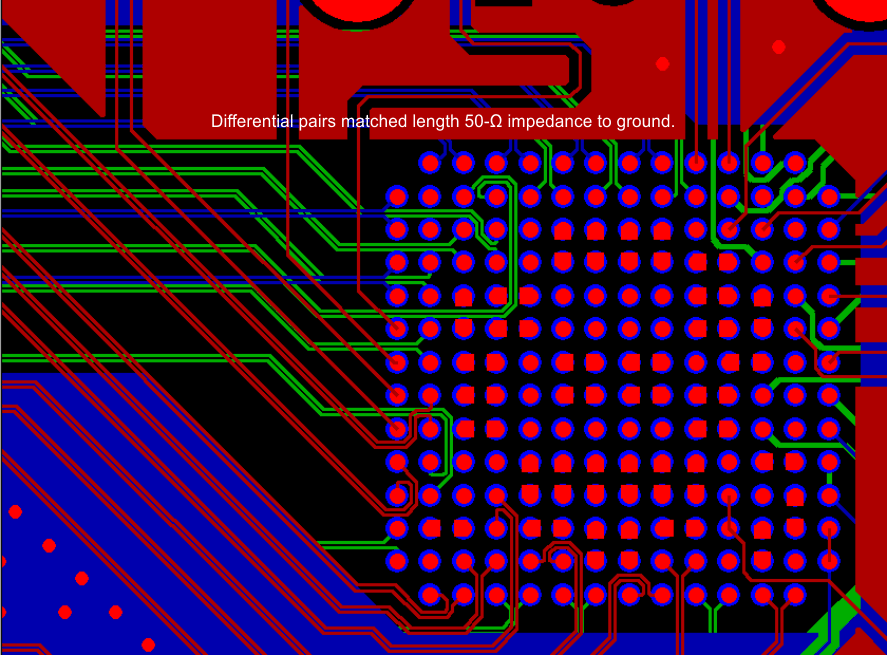
11 Layout
11.1 Layout Guidelines
- DAC output termination should be placed as close as possible to outputs.
- Keep routing for RBIAS short.
- Decoupling capacitors should be placed as close as possible to supply pins.
- Digital differential inputs must be 50 Ω to ground loosely coupled, or 100-Ω differential tightly coupled.
- Digital differential inputs must be length matched.
11.2 Layout Example