SBAS794E november 2018 – august 2023 DAC60501 , DAC70501 , DAC80501
PRODUCTION DATA
- 1
- 1 Features
- 2 Applications
- 3 Description
- 4 Revision History
- 5 Device Comparison Table
- 6 Pin Configuration and Functions
-
7 Specifications
- 7.1 Absolute Maximum Ratings
- 7.2 ESD Ratings
- 7.3 Recommended Operating Conditions
- 7.4 Thermal Information
- 7.5 Electrical Characteristics
- 7.6 Timing Requirements: SPI Mode
- 7.7 Timing Requirements: I2C Standard Mode
- 7.8 Timing Requirements: I2C Fast Mode
- 7.9 Timing Requirements: I2C Fast-Mode Plus
- 7.10 Timing Diagrams
- 7.11 Typical Characteristics
- 8 Detailed Description
- 9 Application and Implementation
- 10Device and Documentation Support
- 11Mechanical, Packaging, and Orderable Information
Package Options
Mechanical Data (Package|Pins)
Thermal pad, mechanical data (Package|Pins)
Orderable Information
3 Description
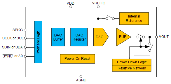
The 16-bit DAC80501, 14-bit DAC70501, and 12-bit DAC60501 (DACx0501) digital-to-analog converters (DACs) are highly accurate, low-power devices with voltage-output. The DACx0501 are specified monotonic by design, and offer linearity of < 1 LSB. These devices include a 2.5-V, 5-ppm/°C internal reference, giving full-scale output voltage ranges of 1.25 V, 2.5 V, or 5 V. The DACx0501 incorporate a power-on-reset (POR) circuit that makes sure the DAC output powers up at zero scale or midscale, and remains at that scale until a valid code is written to the device. These devices consume a low current of 1 mA, and include a power-down feature that reduces current consumption to typically 15 µA at 5 V.
The digital interface of the DACx0501 can be configured to SPI or I2C mode using the SPI2C pin. In SPI mode, the DACx0501 use a versatile 3-wire serial interface that operates at clock rates of up to 50 MHz. In I2C mode, the DACx0501 operate in standard mode (100Kbps), fast mode (400Kbps), and fast mode plus (1.0Mbps).
| PART NUMBER(1) | RESOLUTION | PACKAGE(2) |
|---|---|---|
| DAC80501 | 16-bit | WSON (8) |
| VSSOP (10) | ||
| DAC70501 | 14-bit | WSON (8) |
| VSSOP (10) | ||
| DAC60501 | 12-bit | WSON (8) |
| VSSOP (10) |
 Functional Block
Diagram
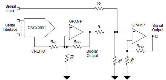
 Offset Trimming With the
DACx0501