SBAS793A November   2019  – April 2020 DAC60502 , DAC70502 , DAC80502

PRODUCTION DATA.  

  1. Features
  2. Applications
  3. Description
    1.     Device Images
      1.      Functional Block Diagram
  4. Revision History
  5. Device Comparison Table
  6. Pin Configuration and Functions
    1.     Pin Functions
  7. Specifications
    1. 7.1  Absolute Maximum Ratings
    2. 7.2  ESD Ratings
    3. 7.3  Recommended Operating Conditions
    4. 7.4  Thermal Information
    5. 7.5  Electrical Characteristics
    6. 7.6  Timing Requirements : SPI Mode
    7. 7.7  Timing Requirements : I2C Standard Mode
    8. 7.8  Timing Requirements : I2C Fast Mode
    9. 7.9  Timing Requirements : I2C Fast-Mode Plus
    10. 7.10 Typical Characteristics
  8. Detailed Description
    1. 8.1 Overview
    2. 8.2 Functional Block Diagram
    3. 8.3 Feature Description
      1. 8.3.1 Digital-to-Analog Converter (DAC) Architecture
        1. 8.3.1.1 DAC Transfer Function
        2. 8.3.1.2 DAC Register Structure
        3. 8.3.1.3 Output Amplifier
      2. 8.3.2 Internal Reference
        1. 8.3.2.1 Solder Heat Reflow
      3. 8.3.3 Power-On Reset (POR)
      4. 8.3.4 Software Reset
    4. 8.4 Device Functional Modes
      1. 8.4.1 Power-Down Mode
    5. 8.5 Programming
      1. 8.5.1 Serial Interface
        1. 8.5.1.1 SPI Mode
          1. 8.5.1.1.1 SYNC Interrupt
        2. 8.5.1.2 I2C Mode
          1. 8.5.1.2.1 F/S Mode Protocol
          2. 8.5.1.2.2 DACx0502 I2C Update Sequence
            1. 8.5.1.2.2.1 DACx0502 Address Byte
            2. 8.5.1.2.2.2 DACx0502 Command Byte
            3. 8.5.1.2.2.3 DACx0502 Data Byte (MSDB and LSDB)
          3. 8.5.1.2.3 DACx0502 I2C Read Sequence
    6. 8.6 Register Maps
      1. 8.6.1 Registers
        1. 8.6.1.1 NOOP Register (offset = 0h) [reset = 0000h]
          1. Table 9. NOOP Register Field Descriptions
        2. 8.6.1.2 DEVID Register (offset = 1h) [reset = 0214h for DAC80502, 1214h for DAC70502, 2214h for DAC60502]
          1. Table 10. DEVID Register Field Descriptions
        3. 8.6.1.3 SYNC Register (offset = 2h) [reset = 0300h]
          1. Table 11. SYNC Register Field Descriptions
        4. 8.6.1.4 CONFIG Register (offset = 3h) [reset = 0000h]
          1. Table 12. CONFIG Register Field Descriptions
        5. 8.6.1.5 GAIN Register (offset = 4h) [reset = 0003h]
          1. Table 13. GAIN Register Field Descriptions
        6. 8.6.1.6 TRIGGER Register (offset = 5h) [reset = 0000h]
          1. Table 14. TRIGGER Register Field Descriptions
        7. 8.6.1.7 BRDCAST Register (offset = 6h) [reset = 0000h for RSTSEL = 0, or reset = 8000h for RSTSEL = 1]
          1. Table 15. BRDCAST Register Field Descriptions
        8. 8.6.1.8 STATUS Register (offset = 7h) [reset = 0000h]
          1. Table 16. STATUS Register Field Descriptions
        9. 8.6.1.9 DAC-n Register (offset = 8h–9h) [reset = 0000h for RSTSEL = 0, or reset = 8000h for RSTSEL = 1]
          1. Table 17. DAC-A Data Register Field Descriptions (8h)
          2. Table 18. DAC-B Data Register Field Descriptions (9h)
  9. Application and Implementation
    1. 9.1 Application Information
    2. 9.2 Typical Application
      1. 9.2.1 Design Requirements
      2. 9.2.2 Detailed Design Procedure
      3. 9.2.3 Application Curves
    3. 9.3 System Examples
      1. 9.3.1 SPI Connection to a Processor
      2. 9.3.2 I2C Interface Connection to a Processor
    4. 9.4 What To Do and What Not To Do
      1. 9.4.1 What To Do
      2. 9.4.2 What Not To Do
    5. 9.5 Initialization Setup
  10. 10Power Supply Recommendations
  11. 11Layout
    1. 11.1 Layout Guidelines
    2. 11.2 Layout Example
  12. 12Device and Documentation Support
    1. 12.1 Documentation Support
      1. 12.1.1 Related Documentation
    2. 12.2 Related Links
    3. 12.3 Receiving Notification of Documentation Updates
    4. 12.4 Support Resources
    5. 12.5 Trademarks
    6. 12.6 Electrostatic Discharge Caution
    7. 12.7 Glossary
  13. 13Mechanical, Packaging, and Orderable Information

Package Options

Mechanical Data (Package|Pins)
Thermal pad, mechanical data (Package|Pins)
Orderable Information

SYNC Interrupt

For SPI-mode operation, the SYNC line stays low for at least 24 falling edges of SCLK, and the addressed DAC register updates on the SYNC rising edge. However, if the SYNC line is brought high before the 24th SCLK falling edge, this event acts as an interrupt to the write sequence. The shift register resets and the write sequence is discarded. The data buffer contents and the DAC register contents do not update, and the the operating mode does not change, as shown in Figure 58.
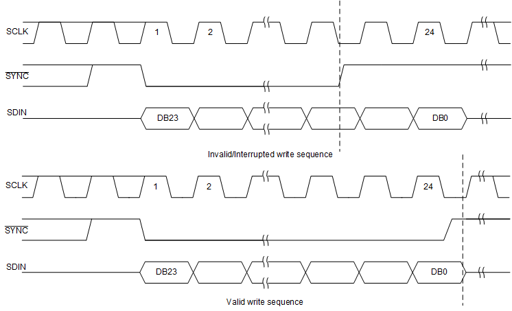
DAC80502 DAC70502 DAC60502 SBAS793_DACx0502_SYNC_Interrupt.gifFigure 58. SYNC Interrupt