SBAS439C August 2008 – July 2015 DAC8311 , DAC8411
PRODUCTION DATA.
- 1 Features
- 2 Applications
- 3 Description
- 4 Revision History
- 5 Device Comparison
- 6 Pin Configuration and Functions
- 7 Specifications
- 8 Detailed Description
- 9 Application and Implementation
- 10Power Supply Recommendations
- 11Layout
- 12Device and Documentation Support
- 13Mechanical, Packaging, and Orderable Information
Package Options
Mechanical Data (Package|Pins)
- DCK|6
Thermal pad, mechanical data (Package|Pins)
Orderable Information
9 Application and Implementation
NOTE
Information in the following applications sections is not part of the TI component specification, and TI does not warrant its accuracy or completeness. TI’s customers are responsible for determining suitability of components for their purposes. Customers should validate and test their design implementation to confirm system functionality.
9.1 Application Information
9.1.1 Microprocessor Interfacing
9.1.1.1 DAC8x11 to 8051 Interface
Figure 81 shows a serial interface between the DAC8x11 and a typical 8051-type microcontroller. The setup for the interface is as follows: TXD of the 8051 drives SCLK of the DAC8x11, while RXD drives the serial data line of the part. The SYNC signal is derived from a bit programmable pin on the port. In this case, port line P3.3 is used. When data are to be transmitted to the DAC8x11, P3.3 is taken low. The 8051 transmits data only in 8-bit bytes; thus, only eight falling clock edges occur in the transmit cycle. To load data to the DAC, P3.3 remains low after the first eight bits are transmitted, and a second write cycle is initiated to transmit the second byte of data. P3.3 is taken high following the completion of this cycle. The 8051 outputs the serial data in a format which has the LSB first. The DAC8x11 requires its data with the MSB as the first bit received. Therefore, the 8051 transmit routine must take this requirement into account, and mirror the data as needed.
 Figure 81. DAC8x11 to 80C51/80l51 Interfaces
9.1.1.2 DAC8x11 to Microwire Interface
Figure 82 shows an interface between the DAC8x11 and any Microwire-compatible device. Serial data are shifted out on the falling edge of the serial clock and are clocked into the DAC8x11 on the rising edge of the SK signal.
 Figure 82. DAC8x11 to Microwire Interface
9.1.1.3 DAC8x11 to 68HC11 Interface
Figure 83 shows a serial interface between the DAC8x11 and the 68HC11 microcontroller. SCK of the 68HC11 drives the SCLK of the DAC8x11, while the MOSI output drives the serial data line of the DAC. The SYNC signal is derived from a port line (PC7), similar to what was done for the 8051.
 Figure 83. DAC8X11 to 68HC11 Interface
The 68HC11 should be configured so that its CPOL bit is a '0' and its CPHA bit is a '1'. This configuration causes data appearing on the MOSI output to be valid on the falling edge of SCK. When data are being transmitted to the DAC, the SYNC line is taken low (PC7). Serial data from the 68HC11 are transmitted in 8-bit bytes with only eight falling clock edges occurring in the transmit cycle. Data are transmitted MSB first. In order to load data to the DAC8x11, PC7 is held low after the first eight bits are transferred, and a second serial write operation is performed to the DAC; PC7 is taken high at the end of this procedure.
9.2 Typical Applications
9.2.1 Loop Powered Transmitter
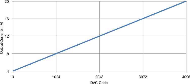
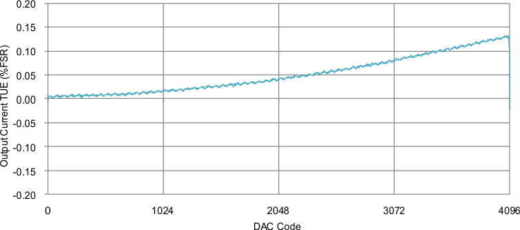
The described loop powered transmitter can accurately source currents from 4 mA to 20 mA.
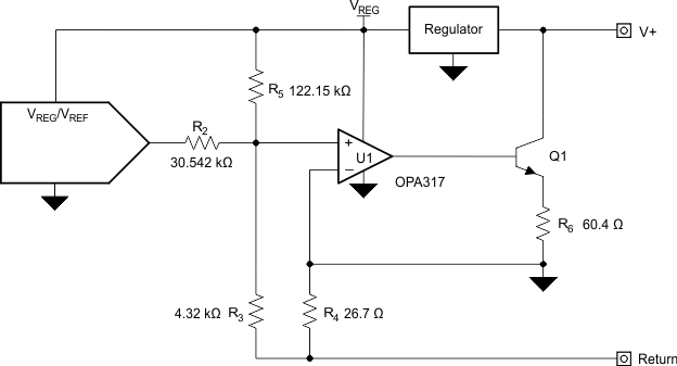 Figure 84. Loop Powered Transmitter Schematic
9.2.1.1 Design Requirements
The transmitter has only two external input terminals; a supply connection and a ground (or return) connection. The transmitter communicates back to the host, typically a PLC analog input module, by precisely controlling the magnitude of the return current. In order to conform to the 4-mA to 20-mA communication standards, the complete transmitter must consume less than 4 mA of current.
The complete design of this circuit is outlined in TIPD158, Low Cost Loop-Powered 4-20mA Transmitter EMC/EMI Tested Reference Design. The design is expected to be low-cost and deliver immunity to the IEC61000-4 suite of tests with minimum impact on the accuracy of the system. Reference design TIPD158 includes the design goals, simulated results, and measured performance.
9.2.1.2 Detailed Design Procedure
Amplifier U1 uses negative feedback to make sure that the potentials at the inverting (V–) and noninverting (V+) input terminals are equal. In this configuration, V– is directly tied to the local GND; therefore, the potential at the noninverting input terminal is driven to local ground. Thus, the voltage difference across R2 is the DAC output voltage (VOUT), and the voltage difference across R5 is the regulator voltage (VREG). These voltage differences cause currents to flow through R2 and R5, as illustrated in Figure 85.
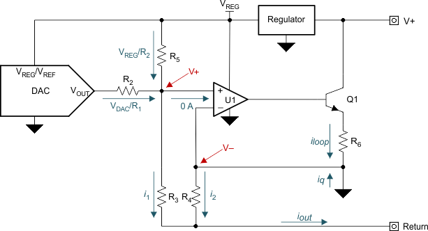 Figure 85. Voltage to Current Conversion
The currents from R2 and R5 sum into i1 (defined in Equation 1), and i1 flows through R3.

Amplifier U2 drives the base of Q1, the NPN bipolar junction transistor (BJT), to allow current to flow through R4 so that the voltage drops across R3 and R4 remain equal. This design keeps the inverting and noninverting terminals at the same potential. A small part of the current through R4 is sourced by the quiescent current of all of the components used in the transmitter design (regulator, amplifier, and DAC). The voltage drops across R3 and R4 are equal; therefore, different-sized resistors cause different current flow through each resistor. Use these different-sized resistors to apply gain to the current flow through R4 by controlling the ratio of resistor R3 to R4, as shown in Equation 2:

The current gain in the circuit helps allow a majority of the output current to come directly from the loop through Q1 instead of from the voltage-to-current converter. This current gain, in addition to the low-power components, keeps the current consumption of the voltage-to-current converter low. Currents i1 and i2 sum to form output current iout, as shown in Equation 3:

The complete transfer function, arranged as a function of input code, is shown in Equation 4. The remaining sections divide this circuit into blocks for simplified discussion.

Resistor R6 is included to reduce the gain of transistor Q1, and therefore, reduce the closed-loop gain of the voltage-to-current converter for a stable design. Size resistors R2, R3, R4, and R5 based on the full-scale range of the DAC, regulator voltage, and the desired current output range of the design.
9.2.2 Using the REF5050 as a Power Supply for the DAC8x11
As a result of the extremely low supply current required by the DAC8x11, an alternative option is to use a REF5050 5 V precision voltage reference to supply the required voltage to the part, as shown in Figure 88. This option is especially useful if the power supply is too noisy or if the system supply voltages are at some value other than 5 V. The REF5050 outputs a steady supply voltage for the DAC8x11. If the REF5050 is used, the current needed to supply DAC8x11 is typically 110 μA at 5V, with no load on the output of the DAC. When the DAC output is loaded, the REF5050 also needs to supply the current to the load. The total current required (with a 5-kΩ load on the DAC output) is:
110 μA + (5 V / 5 kΩ) = 1.11 mA
The load regulation of the REF5050 is typically 0.002%/mA, resulting in an error of 90 μV for the 1.1 -mA current drawn from it. This value corresponds to a 1.1 LSB error at 16bit (DAC8411).
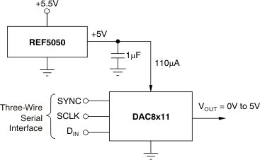 Figure 88. REF5050 as Power Supply to DAC8x11
For other power-supply voltages, alternative references such as the REF3030 (3 V), REF3033 (3.3 V), or REF3220 (2.048 V) are recommended. For a full list of available voltage references from TI, see TI web site at www.ti.com.
9.2.3 Bipolar Operation Using the DAC8x11
The DAC8x11 has been designed for single-supply operation but a bipolar output range is also possible using the circuit in Figure 89. The circuit shown gives an output voltage range of ±5V. Rail-to-rail operation at the amplifier output is achievable using an OPA211, OPA340, or OPA703 as the output amplifier. For a full list of available operational amplifiers from TI, see TI web site at www.ti.com
The output voltage for any input code can be calculated as follows:

where
- n = resolution in bits; either 14 (DAC8311) or 16 (DAC8411).
- D = the input code in decimal; either 0 to 16,383 (DAC8311) or 0 to 65,535 (DAC8411).
With AVDD = 5 V, R1 = R2 = 10 kΩ:

The resulting output voltage range is ±5V. Code 000h corresponds to a –5-V output and FFFFh (16-bit level) corresponding to a 5-V output.
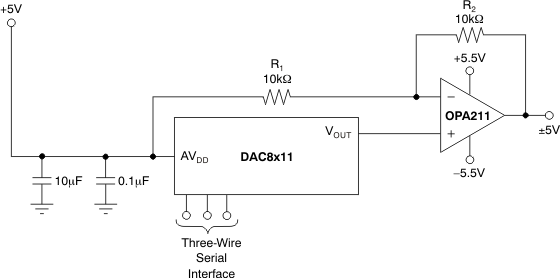 Figure 89. Bipolar Operation With the DAC8x11
