SLASEB8C February 2016 – November 2016 DAC6551-Q1 , DAC8551-Q1
PRODUCTION DATA.
- 1 Features
- 2 Applications
- 3 Description
- 4 Revision History
- 5 Pin Configuration and Functions
- 6 Specifications
- 7 Detailed Description
- 8 Application and Implementation
- 9 Power Supply Recommendations
- 10Layout
- 11Device and Documentation Support
- 12Mechanical, Packaging, and Orderable Information
Package Options
Mechanical Data (Package|Pins)
- DGK|8
Thermal pad, mechanical data (Package|Pins)
Orderable Information
1 Features
- Qualified for Automotive Applications
- AEC-Q100 Qualified With the Following Results:
- Device Temperature Grade 1: –40°C to 125°C Ambient Operating Temperature Range
- Device HBM ESD Classification Level 2
- Device CDM ESD Classification Level C4B
- Relative Accuracy:
- DAC8551-Q1 (16-Bit): 4 LSB INL
- DAC6551-Q1 (12-Bit): 0.3 LSB INL
- Ultralow Glitch Impulse: 0.1 nV-s
- Settling Time: 8 μs to ±0.003% FSR
- Power Supply: 3 V to 5.5 V
- Power-On Reset to Zero Scale
- MicroPower Operation: 160 μA at 5 V
- Low-Power Serial Interface With Schmitt-Triggered Inputs
- On-Chip Output Buffer Amplifier With Rail-to-Rail Operation
- Power-Down Capability
- Binary Input
- SYNC Interrupt Facility
- Available in a Tiny VSSOP-8 Package
2 Applications
- Automotive Radar
- Automotive Sensors
3 Description
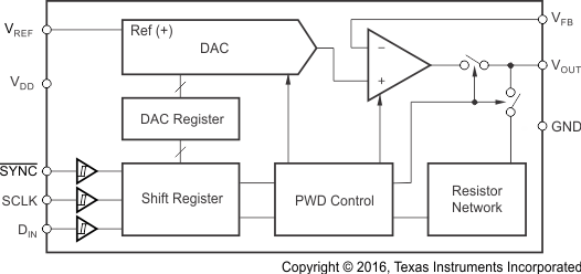
The DAC8551-Q1 and DAC6551-Q1 are small, low-power, voltage-output, 16- and 12-bit digital-to-analog converters (DACs) qualified for automotive applications. The DACx551-Q1 devices provide good linearity and minimize undesired code-to-code transient voltages. The devices use a versatile 3-wire serial interface that operates at clock rates to 30 MHz and is compatible with standard SPI, QSPI, Microwire, and digital signal-processor (DSP) interfaces.
The DACx551-Q1 devices require an external reference voltage to set the output range. The devices incorporate a power-on-reset circuit that ensures the DAC output powers up at 0 V and remains there until a valid write to the device takes place. The devices contain a power-down feature, accessed over the serial interface, that reduces the current consumption to 800 nA at 5 V.
The DACx551-Q1 devices power consumption is only 800 µW at 5 V, reducing to less than 4 μW in power-down mode. The DACx551-Q1 devices are available in a VSSOP-8 package.
Device Information(1)
| PART NUMBER | PACKAGE | BODY SIZE (NOM) |
|---|---|---|
| DAC8551-Q1 DAC6551-Q1 |
VSSOP (8) | 3.00 mm × 3.00 mm |
- For all available packages, see the orderable addendum at the end of the data sheet.
