DLPS180C may 2020 – july 2023 DLP2010LC
PRODUCTION DATA
- 1
- 1 Features
- 2 Applications
- 3 Description
- 4 Revision History
- 5 Pin Configuration and Functions
-
6 Specifications
- 6.1 Absolute Maximum Ratings
- 6.2 Storage Conditions
- 6.3 ESD Ratings
- 6.4 Recommended Operating Conditions
- 6.5 Thermal Information
- 6.6 Electrical Characteristics
- 6.7 Timing Requirements
- 6.8 Switching Characteristics
- 6.9 System Mounting Interface Loads
- 6.10 Physical Characteristics of the Micromirror Array
- 6.11 Micromirror Array Optical Characteristics
- 6.12 Window Characteristics
- 6.13 Chipset Component Usage Specification
- 6.14 Software Requirements
- 7 Detailed Description
- 8 Application and Implementation
- 9 Power Supply Recommendations
- 10Layout
- 11Device and Documentation Support
- 12Mechanical, Packaging, and Orderable Information
Package Options
Mechanical Data (Package|Pins)
- FQJ|40
Thermal pad, mechanical data (Package|Pins)
Orderable Information
6.7 Timing Requirements
Device electrical characteristics are over Recommended Operating Conditions unless otherwise noted.
| MIN | NOM | MAX | UNIT | |||
|---|---|---|---|---|---|---|
| LPSDR | ||||||
| tR | Rise slew rate(1) | (30% to 80%) × VDD, Figure 6-3 | 1 | 3 | V/ns | |
| tF | Fall slew rate(1) | (70% to 20%) × VDD, Figure 6-3 | 1 | 3 | V/ns | |
| tR | Rise slew rate(2) | (20% to 80%) × VDD, Figure 6-3 | 0.25 | V/ns | ||
| tF | Fall slew rate(2) | (80% to 20%) × VDD, Figure 6-3 | 0.25 | V/ns | ||
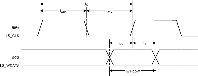
| tC | Cycle time LS_CLK, | Figure 6-2 | 7.7 | 8.3 | ns | |
| tW(H) | Pulse duration LS_CLK high | 50% to 50% reference points, Figure 6-2 | 3.1 | ns | ||
| tW(L) | Pulse duration LS_CLK low | 50% to 50% reference points, Figure 6-2 | 3.1 | ns | ||
| tSU | Setup time | LS_WDATA valid before LS_CLK ↑, Figure 6-2 | 1.5 | ns | ||
| tH | Hold time | LS_WDATA valid after LS_CLK ↑, Figure 6-2 | 1.5 | ns | ||
| tWINDOW | Window time(1)(3) | Setup time + Hold time, Figure 6-2 | 3.0 | ns | ||
| tDERATING | Window time derating(1)(3) | For each 0.25 V/ns reduction in slew rate below 1 V/ns, Figure 6-6 | 0.35 | ns | ||
| SubLVDS | ||||||
| tR | Rise slew rate | 20% to 80% reference points, Figure 6-5 | 0.7 | 1 | V/ns | |
| tF | Fall slew rate | 80% to 20% reference points, Figure 6-5 | 0.7 | 1 | V/ns | |
| tC | Cycle time LS_CLK, | Figure 6-7 | 1.61 | 1.67 | ns | |
| tW(H) | Pulse duration DCLK high | 50% to 50% reference points, Figure 6-7 | 0.71 | ns | ||
| tW(L) | Pulse duration DCLK low | 50% to 50% reference points, Figure 6-7 | 0.71 | ns | ||
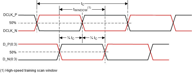
| tSU | Setup time | D(0:3) valid before DCLK ↑ or DCLK ↓, Figure 6-7 | ||||
| tH | Hold time | D(0:3) valid after DCLK ↑ or DCLK ↓, Figure 6-7 | ||||
| tWINDOW | Window time | Setup time + Hold time, Figure 6-7, Figure 6-8 | 3.0 | ns | ||
| tLVDS-ENABLE+REFGEN | Power-up receiver(4) | 2000 | ns | |||
(1) Specification is for LS_CLK and LS_WDATA pins. Refer to LPSDR input rise slew rate and fall slew rate in Figure 6-3.
(2) Specification is for DMD_DEN_ARSTZ pin. Refer to LPSDR input rise and fall slew rate in Figure 6-3.
(3) Window time derating example: 0.5-V/ns slew rate increases the window time by 0.7 ns, from 3 to 3.7 ns.
(4) Specification is for SubLVDS receiver time only and does not take into account commanding and latency after commanding.
A. Low-speed interface is LPSDR and adheres to the
Electrical Characteristics and AC/DC Operating Conditions
table in JEDEC Standard No. 209B, Low Power Double Data Rate (LPDDR)JESD209B.
Figure 6-2 LPSDR Switching Parameters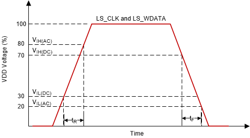 Figure 6-3 LPSDR Input Slew Rate
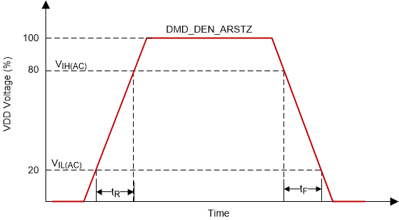 Figure 6-4 LPSDR Input Slew Rate
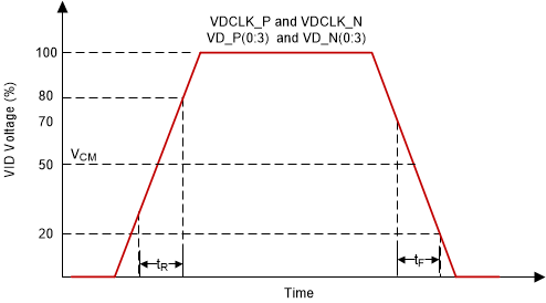 Figure 6-5 SubLVDS Input Rise and Fall Slew Rate
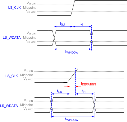 Figure 6-6 Window Time Derating Concept
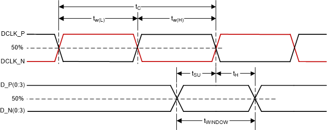 Figure 6-7 SubLVDS Switching Parameters
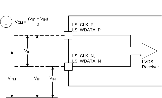 Figure 6-9 SubLVDS Voltage Parameters
A. VSubLVDS(max) = VCM(max) + | ½ × VID(max) |
B. VSubLVDS(min) = VCM(min) – | ½ × VID(max) |
Figure 6-10 SubLVDS Waveform Parameters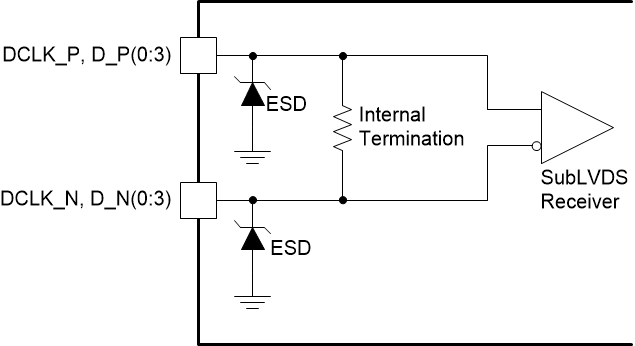 Figure 6-11 SubLVDS Equivalent Input Circuit
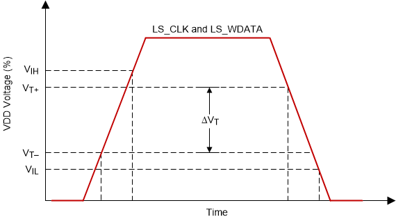 Figure 6-12 LPSDR Input Hysteresis
 Figure 6-13 LPSDR Read Out