DLPS101B November 2017 – February 2023 DLP550JE
PRODUCTION DATA
- 1 Features
- 2 Applications
- 3 Description
- 4 Revision History
- 5 Pin Configuration and Functions
-
6 Specifications
- 6.1 Absolute Maximum Ratings
- 6.2 Storage Conditions
- 6.3 ESD Ratings
- 6.4 Recommended Operating Conditions
- 6.5 Thermal Information
- 6.6 Electrical Characteristics
- 6.7 Timing Requirements
- 6.8 Window Characteristics
- 6.9 System Mounting Interface Loads
- 6.10 Micromirror Array Physical Characteristics
- 6.11 Micromirror Array Optical Characteristics
- 6.12 Chipset Component Usage Specification
- 7 Detailed Description
- 8 Application and Implementation
- 9 Power Supply Recommendations
- 10Device and Documentation Support
- 11Mechanical, Packaging, and Orderable Information
Package Options
Mechanical Data (Package|Pins)
- FYA|149
Thermal pad, mechanical data (Package|Pins)
Orderable Information
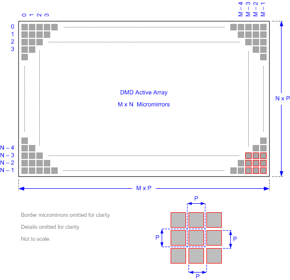
6.10 Micromirror Array Physical Characteristics
| PARAMETER | VALUE | UNIT | |||
|---|---|---|---|---|---|
| Number of active columns#T4989946-27 | M | 1024 | micromirrors | ||
| Number of active rows#T4989946-27 | N | 768 | |||
| Micromirror (pixel) pitch#T4989946-27 | P | 10.8 | µm | ||
| Micromirror active array width#T4989946-27 | Micromirror pitch × number of active columns | 11.059 | mm | ||
| Micromirror active array height #T4989946-27 | Micromirror pitch × number of active columns | 8.294 | mm | ||
| Micromirror active array border#DLPS1016158 | Pond of Micromirror (POM) | 10 | micromirrors/side | ||
(1) See #DLPS1012803.
(2) The structure and qualities of the border around the active
array includes a band of partially functional micromirrors referred to as the
Pond Of Mirrors (POM). These micromirrors are structurally and/or electrically
prevented from tilting toward the bright or ON state, but still require an
electrical bias to tilt toward OFF.

Refer to the
#GUID-1CB02D98-1462-483C-8A3D-44D15A8F121D for M, N, and P specifications.
Figure 6-11 Micromirror Array Physical Characteristics